Clock voltage-multiplying circuit and charge pump

A voltage doubling circuit and clock technology, which is applied to electrical components, output power conversion devices, DC power input conversion to DC power output, etc., can solve problems such as clock voltage doubling circuit abnormality, achieve protection and ensure normal operation Effect

Active Publication Date: 2017-04-26
INST OF MICROELECTRONICS CHINESE ACAD OF SCI
View PDF3 Cites 5 Cited by
  • Summary
  • Abstract
  • Description
  • Claims
  • Application Information

AI Technical Summary

Problems solved by technology

[0006] In order to solve the above technical problems, the present invention provides a clock voltage doubler circuit and a charge pump to solve the problem that the clock voltage doubler circuit functions when the process angle and working conditions of the transistor are relatively harsh and the input operating voltage swing is small. abnormal problem

Method used


Image

  • Clock voltage-multiplying circuit and charge pump
  • Clock voltage-multiplying circuit and charge pump
  • Clock voltage-multiplying circuit and charge pump

Examples


Embodiment Construction

[0031] The following will clearly and completely describe the technical solutions in the embodiments of the present invention with reference to the accompanying drawings in the embodiments of the present invention. Obviously, the described embodiments are only some, not all, embodiments of the present invention. Based on the embodiments of the present invention, all other embodiments obtained by persons of ordinary skill in the art without making creative efforts belong to the protection scope of the present invention.

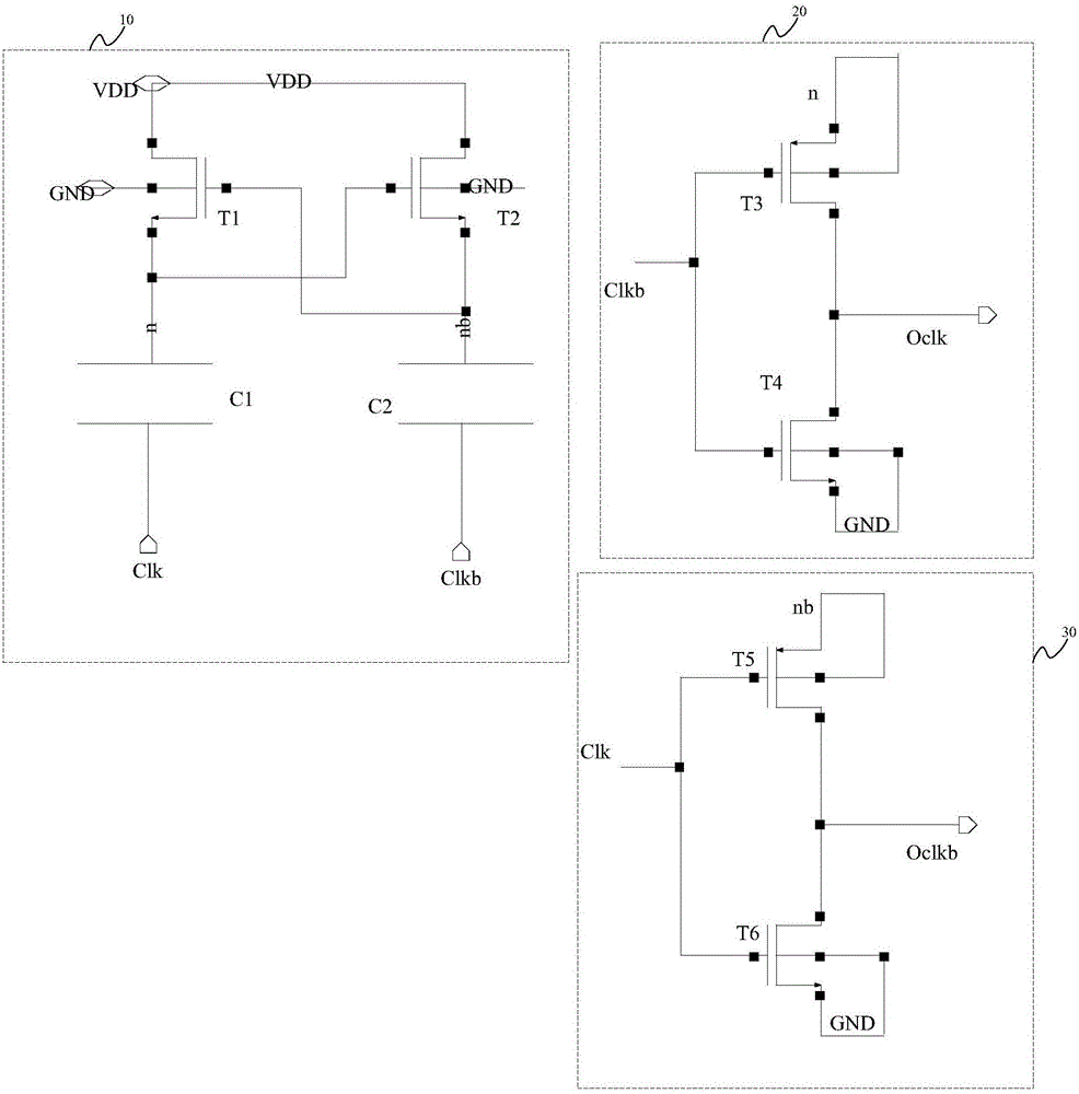
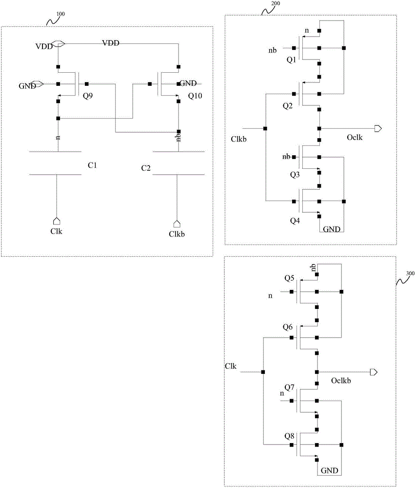
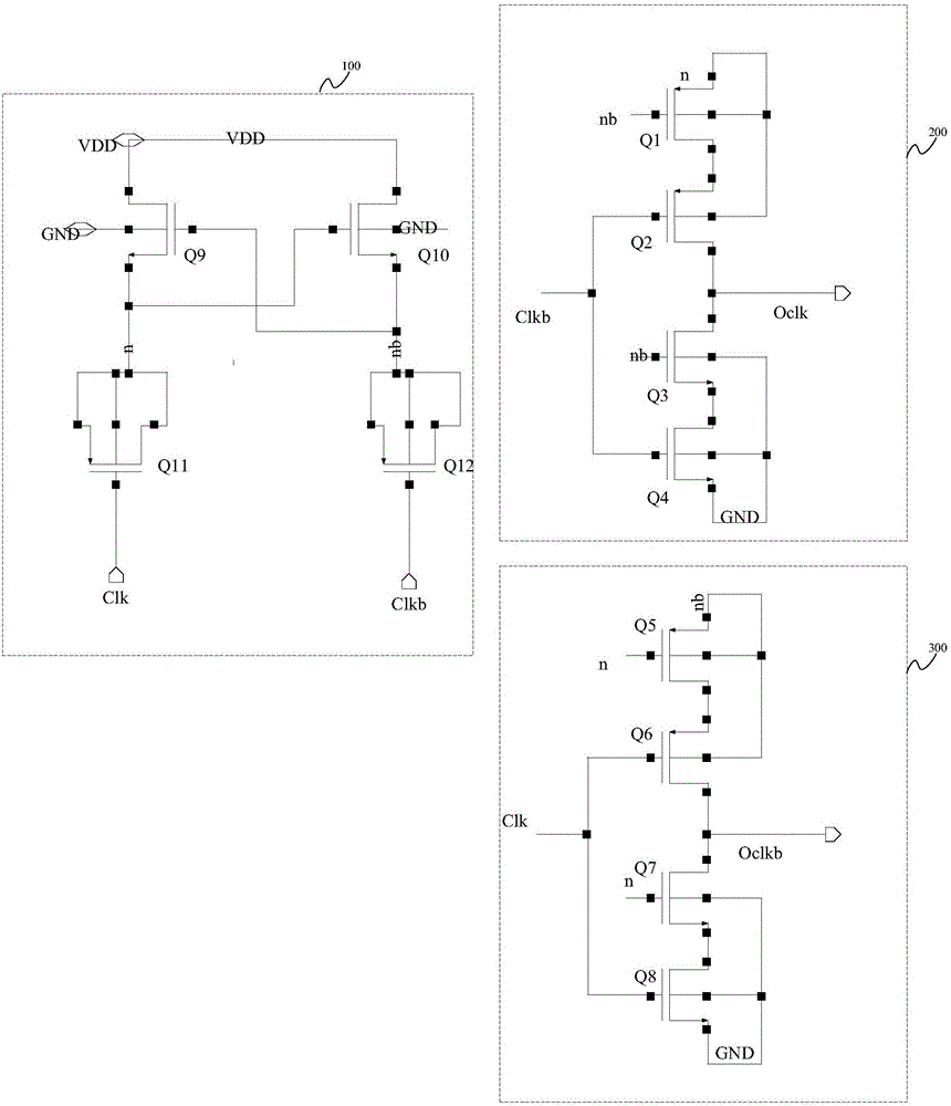
[0032] The embodiment of the present application provides a clock voltage doubling circuit, such as figure 2 As shown, it includes: an input unit 100, a first buffer unit 200 and a second buffer unit 300, wherein,

[0033] The input unit 100 includes a working voltage input terminal, a first clock input terminal, a second clock input terminal, a first voltage output terminal and a second voltage output terminal, wherein the working voltage input terminal is u...


PUM


Abstract

The application discloses a clock voltage-multiplying circuit and a charge pump. The clock voltage-multiplying circuit includes an input unit, a first buffering unit and a second buffering unit. The clock voltage-multiplying circuit connects a second transistor and a third transistor which are input / output devices with a first transistor and a fourth transistor which are logic devices having relatively small threshold values in series, and connects a sixth transistor and seventh transistor which are input / output devices with a fifth transistor and an eighth transistor which are logic devices having relatively small threshold voltage in series, thus when input working voltage swing is relatively small, and when first voltage and second voltage output by an input unit are relatively small, the logic devices with the relatively small threshold values can be normally turned on, thereby ensuring normal turning-on of the input / output devices, enabling the clock voltage-multiplying circuit to work normally, ensuring that a voltage difference between any two poles of the logic device transistors in a working process not to exceed the working voltage, realizing protection of the logic device transistors, and guaranteeing normal work of the clock voltage-multiplying circuit.

Description

technical field [0001] The present application relates to the technical field of clock voltage doubling circuit design, and more specifically, to a clock voltage doubling circuit and a charge pump. Background technique [0002] Charge pumps are widely used in high-voltage devices, and their basic design concept is to couple charge from the charge pump clock to each charge pump node. Higher coupling voltages will result in higher output voltages with fewer charge pump stages. The clock signal is mainly provided for the charge pump through a clock voltage doubler circuit. figure 1 It is a schematic circuit structure diagram of a clock voltage doubling circuit in the prior art. The clock voltage doubling circuit mainly includes an input stage 10, a first buffer stage 20 and a second buffer stage 30, wherein the input stage 10 is composed of a first A capacitor C1, a second capacitor C2, a first transistor T1, and a second transistor T2 are formed. The first buffer stage 20 is...

Claims


Application Information

Patent Timeline
Patent Type & Authority Applications(China)
IPC IPC(8): H02M3/07
CPCH02M3/073H02M1/0041H02M3/075
Inventor 龙煌李弦田敏钟汇才
Owner INST OF MICROELECTRONICS CHINESE ACAD OF SCI
Why Eureka
Try Eureka