Heat-radiation pad, design method thereof and printed circuit board (PCB)

A technology for heat dissipation pads and pads, which is used in printed circuits, printed circuits, and printed circuit manufacturing. , to achieve the effect of preventing tin leakage and improving product quality

Inactive Publication Date: 2017-04-26
ZHEJIANG DAHUA TECH CO LTD
View PDF3 Cites 8 Cited by
  • Summary
  • Abstract
  • Description
  • Claims
  • Application Information

AI Technical Summary

Problems solved by technology

Among them, in the process of printing solder paste, steel mesh is generally used to open holes on the entire heat dissipation pad on the PCB, and use the opening to apply solder paste to the heat dissipation pad; in the process of reflow soldering, it is easy to leak solder paste. There is less tin on the soldering surface in the via hole, which leads to easy soldering of electronic components, which affects product quality. At the same time, solder paste easily passes through the via hole and forms tin beads on the other side of the PCB, which affects the appearance and easily leads to short circuits.

Method used


Image

  • Heat-radiation pad, design method thereof and printed circuit board (PCB)
  • Heat-radiation pad, design method thereof and printed circuit board (PCB)
  • Heat-radiation pad, design method thereof and printed circuit board (PCB)

Examples


Embodiment Construction

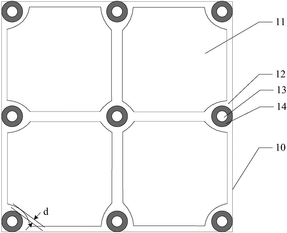
[0033] Embodiments of the present application provide a heat dissipation pad design method, the heat dissipation pad and a printed circuit board, which are used to prevent tin leakage from the heat dissipation pad, thereby improving product quality.

[0034] The following will clearly and completely describe the technical solutions in the embodiments of the application with reference to the drawings in the embodiments of the application. Apparently, the described embodiments are only some of the embodiments of the application, not all of them. All other embodiments obtained by persons of ordinary skill in the art based on the embodiments in this application belong to the protection scope of this application.

[0035] It should be noted that the thickness and shape of each component in the drawings of the present application do not reflect the real scale, and the purpose is only to schematically illustrate the content of the present application.

[0036] It should be pointed ou...


PUM


Abstract

The invention provides a heat-radiation pad, a design method thereof and a PCB, and aims at preventing the heat-radiation pad from tin leakage and improving the product quality. The heat-radiation pad is divided into solder feeding areas independent from each other and a non solder feeding area surrounding all the solder feeding areas; only the non solder feeding area is provided with through holes and through hole pads corresponding to the through holes respectively; and the minimal distance between the edge of each through hole pad and the edge of the adjacent solder feeding area is greater than or equivalent to a preset value.

Description

technical field [0001] The present application relates to the technical field of printed circuit board packaging, in particular to a heat dissipation pad design method, a heat dissipation pad and a printed circuit board. Background technique [0002] With the continuous development of electronic manufacturing technology, the miniaturization of electronic components and the integration of integrated circuits, the heat flux of electronic components and components continues to increase, which brings about the problem of heat dissipation of electronic components. [0003] In order to solve the heat dissipation problem, taking the chip as an example, in the existing design, a large first heat dissipation pad 02 is generally used at the bottom of the chip 01, such as figure 1 As shown, on the top of the printed circuit board 03 (Printed circuit board, PCB), the second heat dissipation pad 04 is set at the corresponding position for welding with the first heat dissipation pad, and ...

Claims


Application Information

Patent Timeline
Patent Type & Authority Applications(China)
IPC IPC(8): H05K1/02H05K1/11H05K3/40
CPCH05K1/0203H05K1/113H05K3/4007H05K2201/06H05K2201/09372
Inventor 周小勇
Owner ZHEJIANG DAHUA TECH CO LTD
Why Eureka
Try Eureka