A kind of optical module and design method thereof

A design method and optical module technology, applied in the field of optical modules, can solve problems such as poor use effect and change, and achieve the effects of good applicability, reduced electromagnetic radiation, and good use effect

Active Publication Date: 2019-05-28
HISENSE BROADBAND MULTIMEDIA TECH
View PDF6 Cites 0 Cited by
  • Summary
  • Abstract
  • Description
  • Claims
  • Application Information

AI Technical Summary

Problems solved by technology

[0006] The purpose of the embodiment of the present invention is to provide an optical module and its design method to solve the problem of the existing optical module. After the coupling capacitor is connected to the high-speed signal line of the PCB board, the impedance on the high-speed signal transmission path will be reduced at the pad. Changes, poor use of the problem

Method used


Image

  • A kind of optical module and design method thereof
  • A kind of optical module and design method thereof
  • A kind of optical module and design method thereof

Examples


Embodiment Construction

[0020] In order to enable those skilled in the art to better understand the technical solutions in the present invention, the technical solutions in the embodiments of the present invention will be clearly and completely described below in conjunction with the drawings in the embodiments of the present invention. Obviously, the described The embodiments are only some of the embodiments of the present invention, not all of them. Based on the embodiments of the present invention, all other embodiments obtained by persons of ordinary skill in the art without making creative efforts shall fall within the protection scope of the present invention.

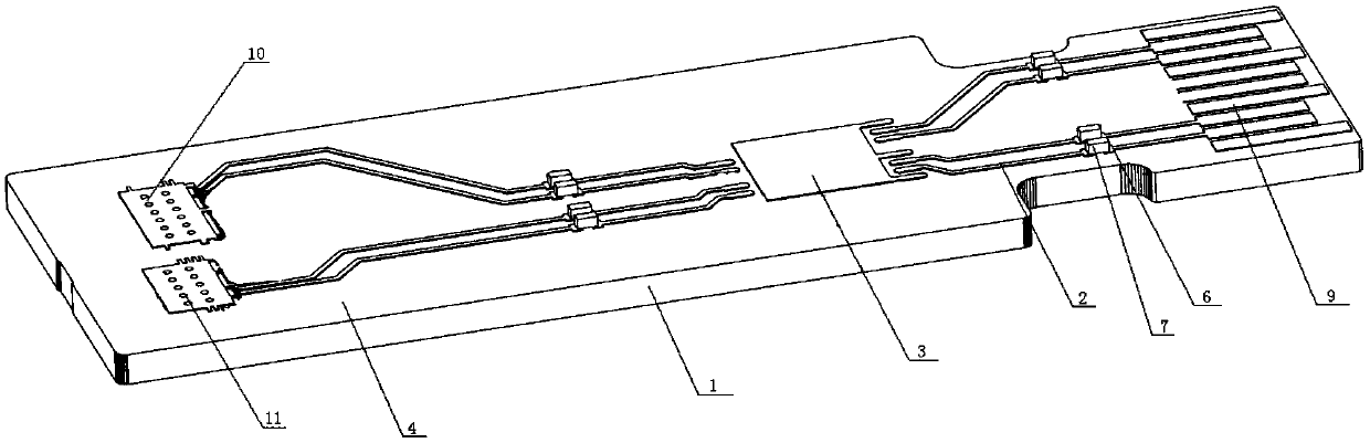
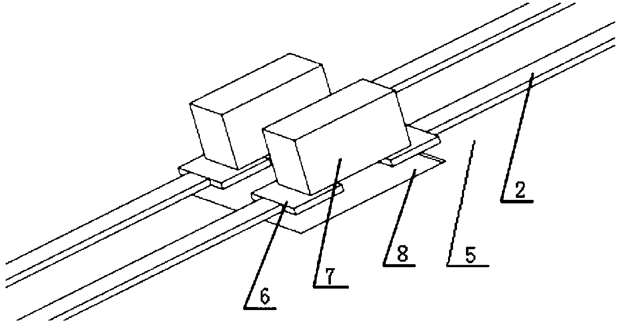
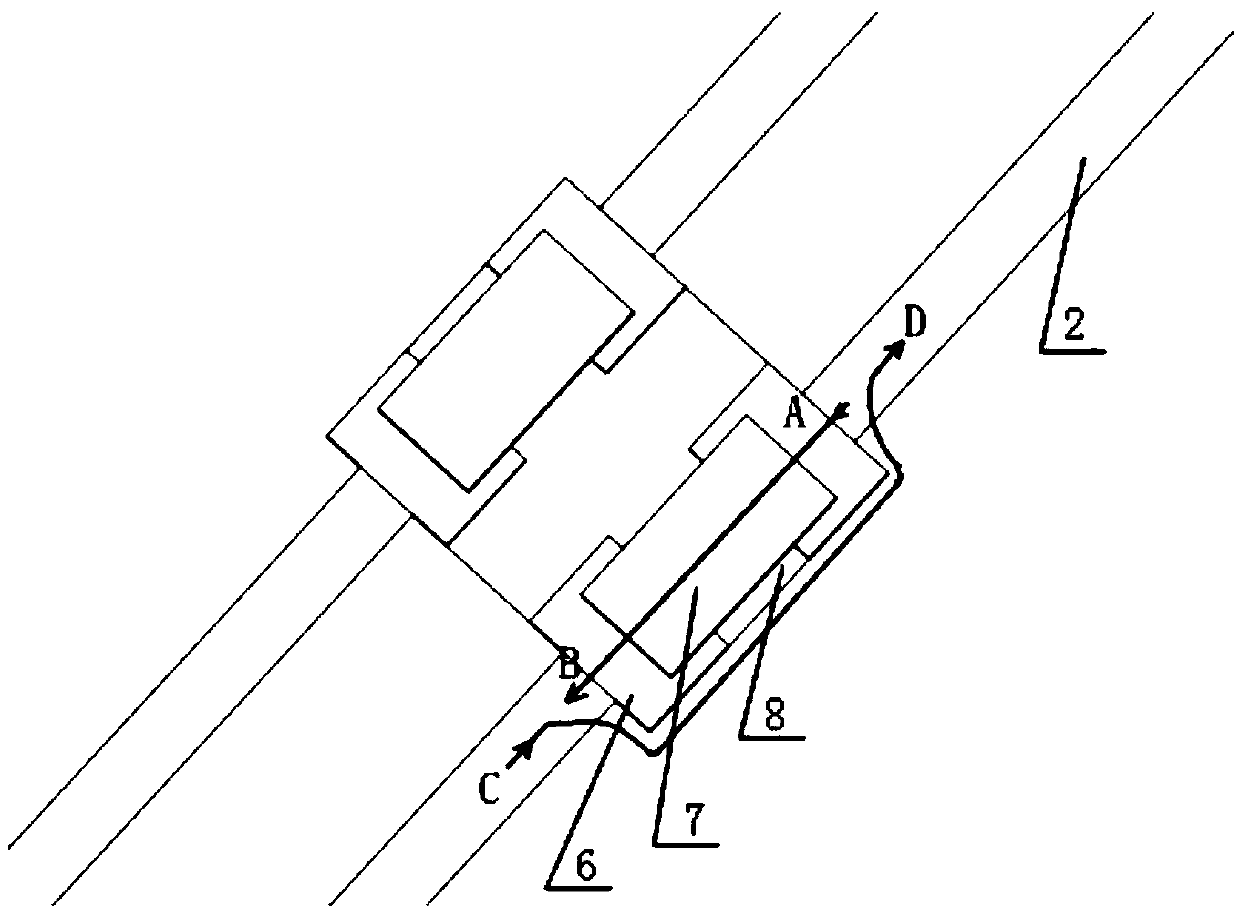
[0021] The present invention provides an optical module and a design method thereof. In the reference reflow layer, the PCB board of the optical module is provided with an insulating area in the area corresponding to the pad above it, which ensures the continuity of the impedance on the transmission path of the high-speed signal. The im...


PUM


Abstract

The invention discloses an optical module and a design method thereof. The optical module comprises: a circuit board, a high-speed signal line, a driving chip and an optical chip; the circuit board comprises a top plate and a metal layer under the top plate, the metal layer is the reference reflow layer of the top board; the driving chip, the high-speed signal line and the optical chip are all arranged on the top board, and the driving chip and the optical chip are connected through the high-speed signal line ; two pads are arranged on the transmission path of the high-speed signal line; the two pads are electrically connected through a coupling capacitor; the projection area of ​​the two pads in the metal layer is provided with an insulating area. In the optical module, the position where the pad is arranged on the high-speed signal line will not undergo sudden change in impedance, and the electromagnetic radiation there is also small, and the applicability is better.

Description

technical field [0001] The invention relates to the technical field of optical modules, in particular to an optical module and a design method thereof. Background technique [0002] At present, with the development of optical communication technology, the single-channel optical fiber rate has been increased from the previous 1G or 10G to the current 25G or 28G. Correspondingly, in order to meet the needs of high-speed development, the PCB of the optical module (that is, the photoelectric converter) (Printed Circuit Board, printed circuit board, referred to as circuit board) The circuit of the board is also designed as a high-speed circuit. [0003] Generally, the PCB board of an optical module includes multiple layers, which are respectively a metal layer and a dielectric layer arranged in an adjacent metal layer. Components, such as a driver chip, are usually arranged on the top metal layer, and are connected to the driver chip. optical chip. In the circuit design of the ...

Claims


Application Information

Patent Timeline
Patent Type & Authority Patents(China)
IPC IPC(8): G02B6/42
CPCG02B6/4277G02B6/428
Inventor 赵伟
Owner HISENSE BROADBAND MULTIMEDIA TECH
Why Eureka
Try Eureka