Printed circuit board patch defect detection method
A defect detection and printed circuit technology, applied in image data processing, instruments, calculations, etc., can solve problems such as large amount of calculation, large background interference, easy to cause misjudgment, etc., to achieve the effect of simple method and comprehensive inspection items
Active Publication Date: 2017-05-10
CHINA AGRI UNIV
View PDF3 Cites 11 Cited by
- Summary
- Abstract
- Description
- Claims
- Application Information
AI Technical Summary
Problems solved by technology
However, traditional image recognition methods, such as image contrast methods, are too sensitive to subtle differences, which can easily lead to misjudgment.
However, other morphological image recognition algorithms, such as wavelet transform and Hough transform, have the disadvantages of large amount of calculation and great influence from background interference, and the detection results cannot fully meet the requirements.
Method used
View moreImage
Smart ImageViewing Examples

Examples
Embodiment
[0154] The implementation process of the present invention is illustrated below by specific examples:
Login to View More PUM
 Abstract
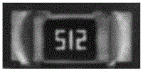
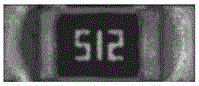
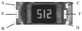
The invention relates to the fields of machine vision and printed circuit board detection, in particular to a machine vision technology-based printed circuit board patch defect detection method. According to the method, identification is performed based on the positions, colors and quantity of pixel points meeting a threshold condition, and an identification algorithm is realized through a relatively small calculation amount. The method comprises the following steps of performing patch locating and size calculation; performing patch region color analysis; and performing patch type identification. The method is simple and convenient; component whole bodies, welding points and patch numbers are identified according to a process; detection items are comprehensive; different detection conditions can be met; and detection programs can be designed for different patches.
Description
technical field [0001] The invention relates to the field of machine vision and the field of printed circuit board detection, in particular to a method for detecting defects of printed circuit board patches based on machine vision technology. Background technique [0002] Circuit boards are an important part of modern industrial products, and product testing is one of the most important processes in the manufacturing process of printed circuit boards. SMD is one of the basic units for modern circuit boards to realize functions. The current development trend of SMT is precision and miniaturization, which requires accurate and high-efficiency printed circuit board (PCB) detection methods. [0003] The pictures taken by ordinary cameras are two-dimensional images, but the surface properties of the solder at both ends of the patch are three-dimensional detection targets. The modern PCB inspection industry widely uses RGB three-color light sources to irradiate the patch, reflec...
Claims
Login to View More Application Information
Patent Timeline
 Patent Type & Authority Applications(China)
IPC IPC(8): G06T7/00G06T7/11G06T5/00
CPCG06T7/0004G06T2207/30141G06T5/70
Inventor 张春龙张淦谭豫之李伟
Owner CHINA AGRI UNIV