Array substrate manufacturing method
An array substrate and glass substrate technology, applied in the field of display panel production, can solve the problems of changing signal line contact, increasing film thickness, affecting adhesion, etc., to achieve the effect of improving display quality, reducing light reflection, and reducing reflection
- Summary
- Abstract
- Description
- Claims
- Application Information
AI Technical Summary
Problems solved by technology
Method used
Image

Examples
Embodiment Construction
[0054] The implementation of the present invention will be described in detail below in conjunction with the accompanying drawings and examples, so as to fully understand and implement the process of how to apply technical means to solve technical problems and achieve technical effects in the present invention. It should be noted that, as long as there is no conflict, each embodiment and each feature in each embodiment of the present invention can be combined with each other, and the formed technical solutions are all within the protection scope of the present invention.
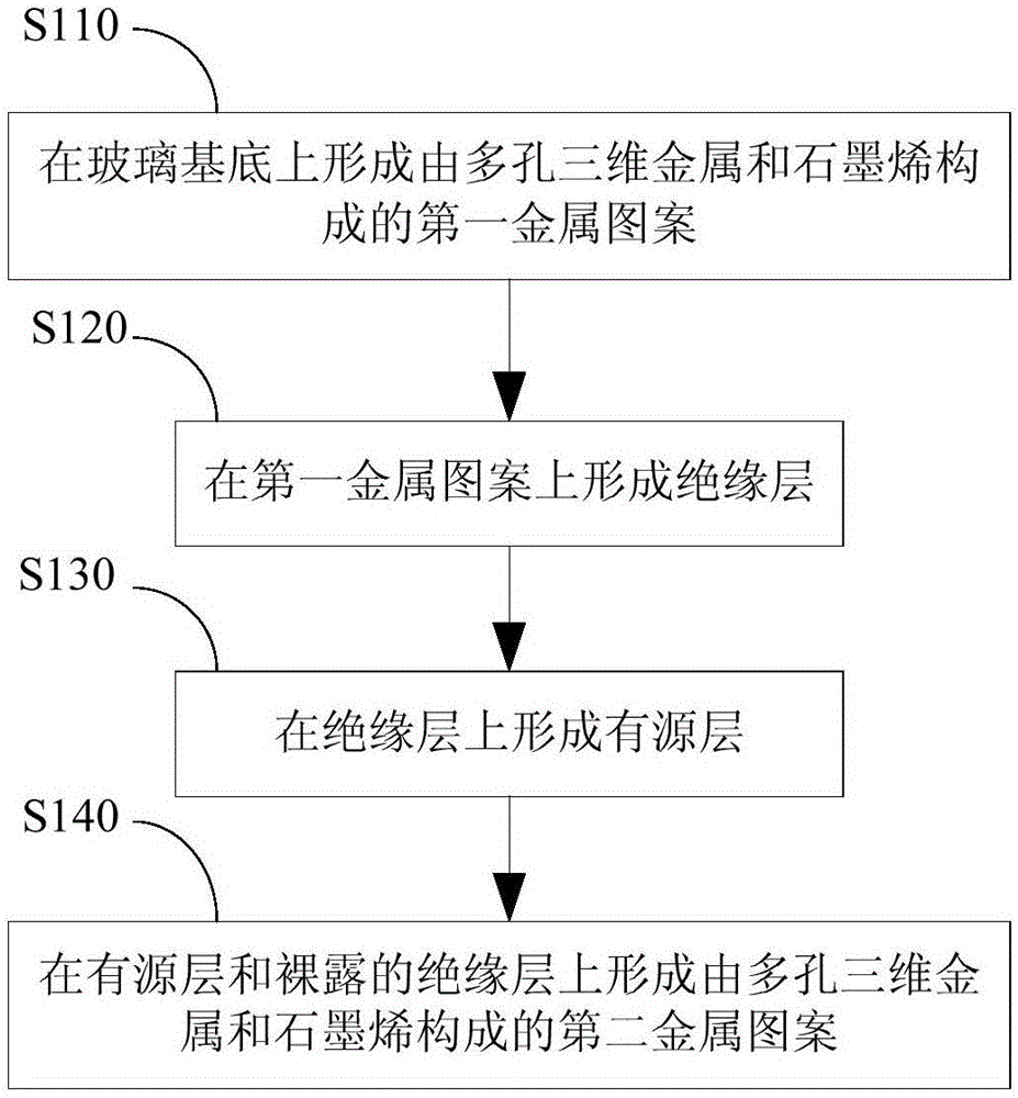
[0055] Such as figure 1 Shown is a flow chart of a method according to an embodiment of the present invention, including: in step S110, forming a first metal pattern made of porous three-dimensional metal and graphene on a glass substrate; in step S120, forming a first metal pattern on the first metal An insulating layer is formed on the pattern; in step S130, an active layer is formed on the insulating laye...
PUM
 Abstract
Description
Claims
Application Information
 - R&D
- Intellectual Property
- Life Sciences
- Materials
- Tech Scout
- Unparalleled Data Quality
- Higher Quality Content
- 60% Fewer Hallucinations
Browse by: Latest US Patents, China's latest patents, Technical Efficacy Thesaurus, Application Domain, Technology Topic, Popular Technical Reports.
© 2025 PatSnap. All rights reserved.Legal|Privacy policy|Modern Slavery Act Transparency Statement|Sitemap|About US| Contact US: help@patsnap.com