
Quantum dot electroluminescent device, and display device and lighting device with quantum dot electroluminescent device

A technology of electroluminescent devices and quantum dots, which is applied in lighting devices, fixed lighting devices, semiconductor devices of light-emitting elements, etc., can solve problems such as carrier injection imbalance, improve luminous efficiency and life, and improve luminous efficiency and working life effects

Inactive Publication Date: 2017-05-10
NANJING TECH CORP LTD
View PDF4 Cites 31 Cited by
  • Summary
  • Abstract
  • Description
  • Claims
  • Application Information

AI Technical Summary

Problems solved by technology

[0007] The main purpose of the present application is to provide a quantum dot electroluminescent device, a display device and a lighting device having it, so as to solve the problem of unbalanced carrier injection in the quantum dot layer in the prior art

Method used


Image

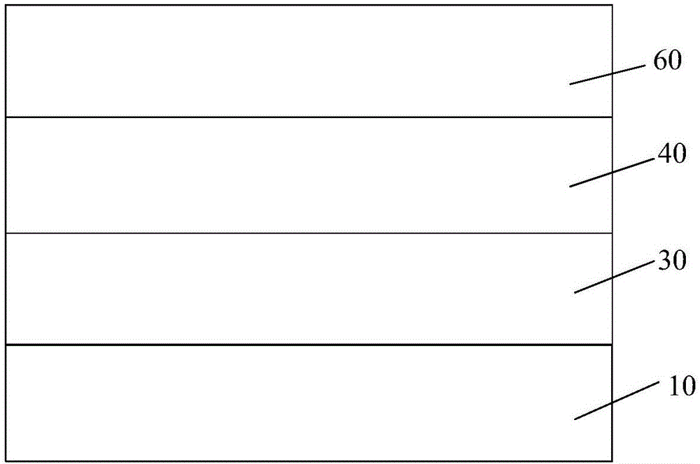
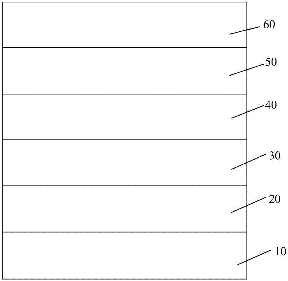
  • Quantum dot electroluminescent device, and display device and lighting device with quantum dot electroluminescent device
  • Quantum dot electroluminescent device, and display device and lighting device with quantum dot electroluminescent device
  • Quantum dot electroluminescent device, and display device and lighting device with quantum dot electroluminescent device

Examples


Embodiment 1

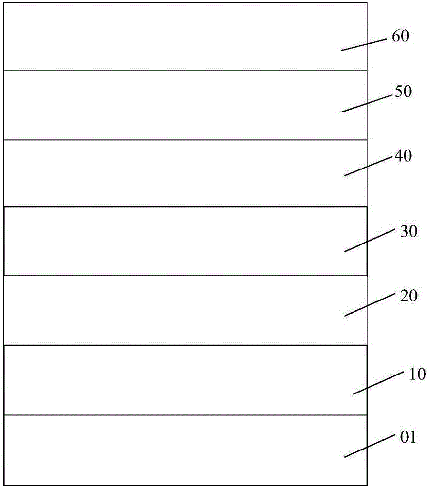
[0062] The structure of quantum dot electroluminescent devices is as follows image 3 As shown, wherein, the substrate 01 is a glass substrate, the material of the anode 10 is ITO, the thickness is 150nm, the material of the quantum dot layer 30 is CdSe / ZnS red core-shell quantum dots, and the wavelength range of its absorption spectrum is between 300-610nm , the thickness of the quantum dot layer 30 is 20nm; the material of the electron blocking layer 40 is a hole transport material, specifically polyvinylcarbazole (PVK), the wavelength range of its fluorescence spectrum is between 380~460nm, and its thickness is 5nm. The absorption spectrum of the dot layer 30 overlaps with the fluorescence spectrum of the electron blocking layer 40; the electronic functional layer 50 is made of ZnO with a thickness of 40nm, and the hole functional layer 20 is poly(3,4-ethylenedioxythiophene)-polystyrene Sulfonic acid PEDOT: PSS and poly(N,N'-bis(4-butylphenyl)-N,N'-bis(phenyl)benzidine) (Po...

Embodiment 2

[0064] The difference from Example 1 is that the thickness of the electron blocking layer 40 is 10 nm.

Embodiment 3

[0066] The difference from Embodiment 2 is that the thickness of the electron blocking layer 40 is 0.1 nm.


PUM

PropertyMeasurementUnit
Thicknessaaaaaaaaaa
Thicknessaaaaaaaaaa
Thicknessaaaaaaaaaa

Abstract

The application provides a quantum dot electroluminescent device, and a display device and a light device with a quantum dot electroluminescent device. The quantum dot electroluminescent device comprises an anode, a quantum dot layer, an electron barrier layer, and a cathode. The quantum dot layer is arranged on the surface of the anode. The electron barrier layer is arranged on the surface, away from the anode, of the quantum dot layer. Materials forming the electron barrier layer include hole transmission materials and / or hole injection materials. The cathode is arranged on the surface, away from the quantum dot layer, of the electron barrier layer. Electrons and the cavity injection quantum dot layer are basically consistent in rate, so that the electrons are close to holes or injection balance is realized during running of the quantum dot electroluminescent device. In this way, quantum dots are electrically neutral, non-radiative recombination, quantum dot charging and the like due to excess electrons in the quantum dots are prevented, and the light-emitting efficiency and the service life of the device are improved.

Description

technical field [0001] The present application relates to the technical field of optoelectronic devices, in particular, to a quantum dot electroluminescence device, a display device and an illumination device having the same. Background technique [0002] Quantum dots are a new type of nano-luminescent material with a diameter in the range of 1-20nm. Due to its small size, the electrons and holes inside it will be restricted in motion, resulting in a quantum confinement effect. The continuous energy band structure becomes a molecular-specific discrete energy level structure. When the quantum dot is excited, Electrons recombine with holes and emit photons after transitioning from the conduction band to the valence band. [0003] With the advancement of quantum dot synthesis technology, the luminous efficiency of quantum dot-based light-emitting devices can be as high as 100%; and the luminous spectrum of quantum dots is easy to adjust, as long as the quantum dot size is chan...

Claims


Application Information

Patent Timeline
IPC IPC(8): H01L51/50G09G3/3208F21S8/00F21Y115/10
CPCF21S8/00H10K50/115H10K50/18
Inventor 陈涛
Owner NANJING TECH CORP LTD
Learn More