

Thin film transistor and display panel
A technology of thin film transistor and polysilicon layer, which is applied in transistors, semiconductor devices, electric solid devices, etc., can solve the problems of complicated manufacturing process and achieve the effect of reducing off-current
- Summary
- Abstract
- Description
- Claims
- Application Information
AI Technical Summary
Problems solved by technology
Method used
Image

Examples
Embodiment Construction
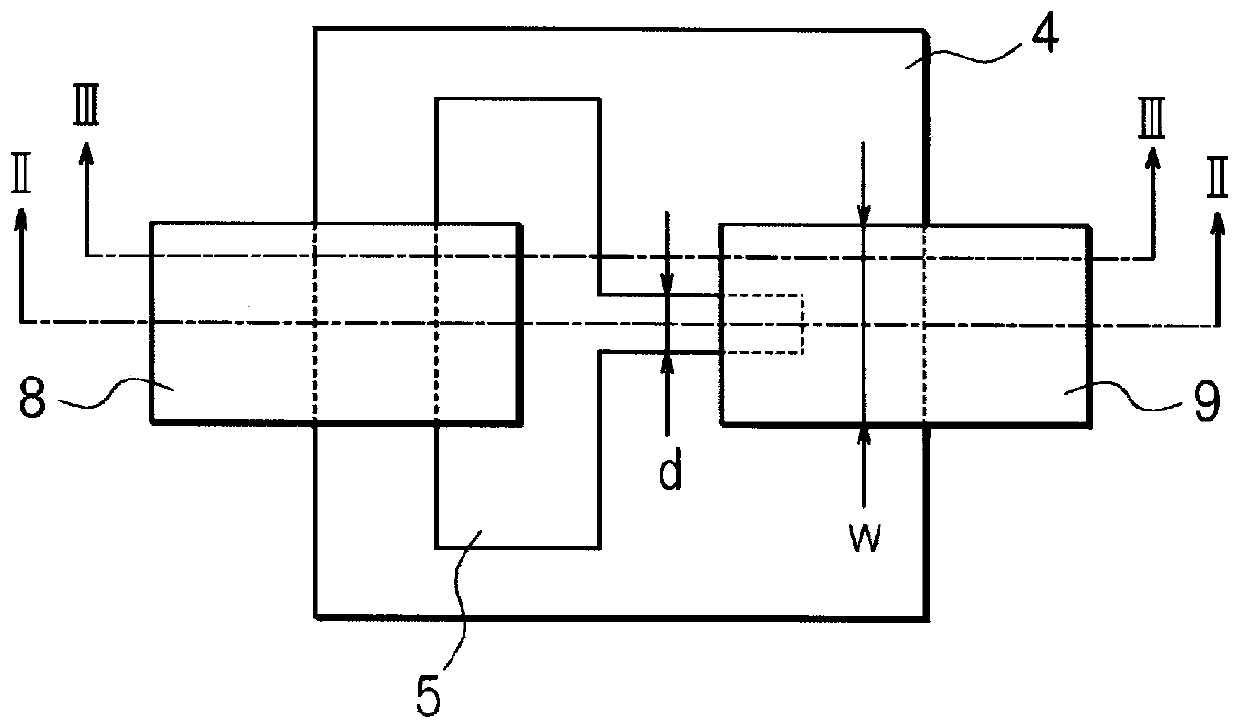
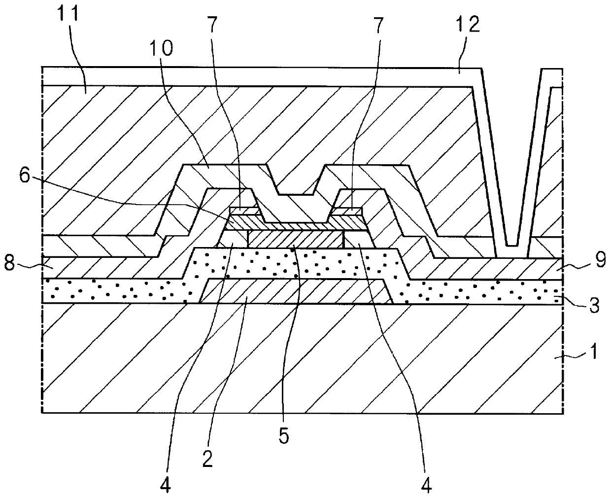
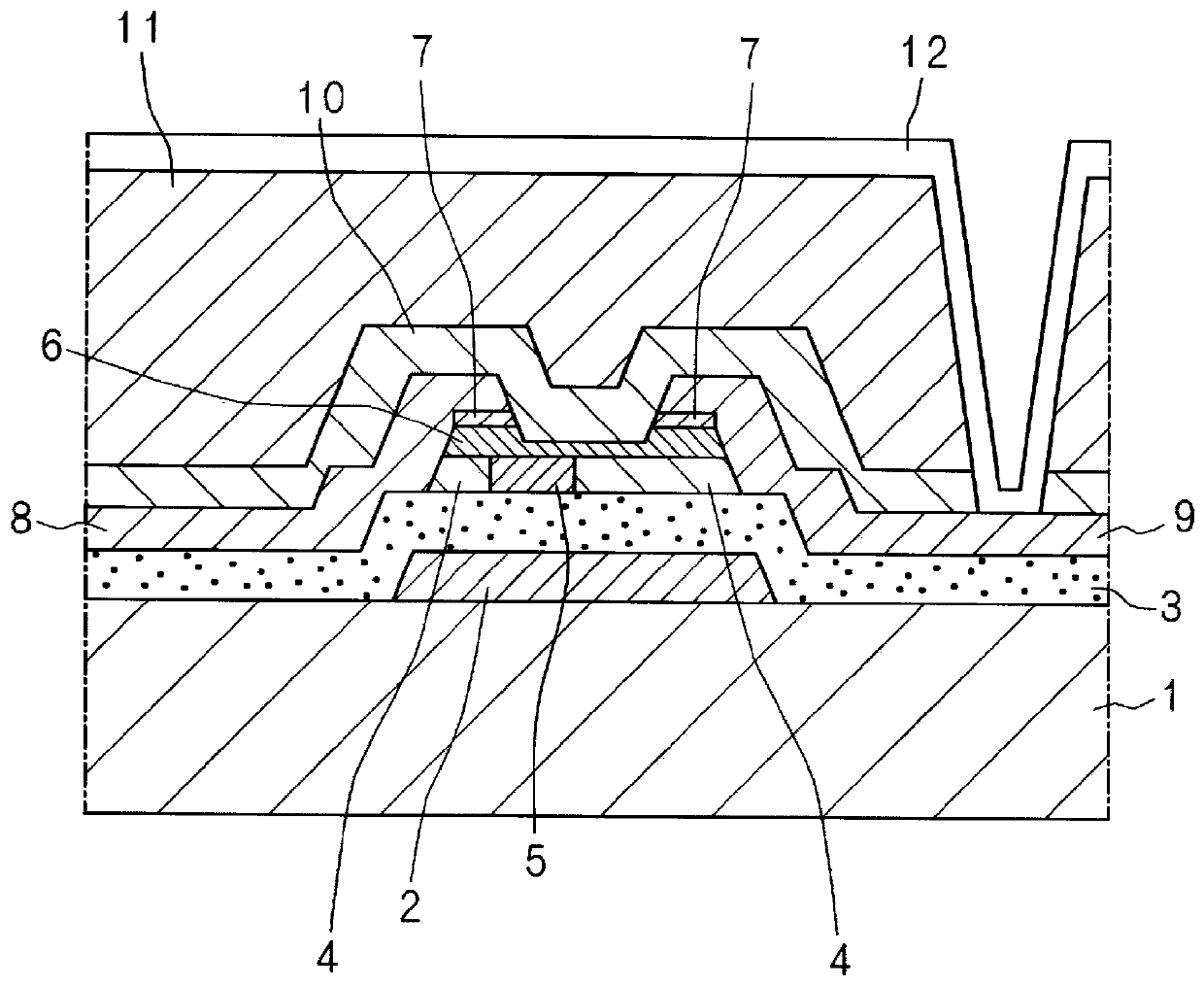
[0044] Hereinafter, the present invention will be described based on drawings showing embodiments of the present invention. figure 1 is a schematic plan view of the main part of the first example showing the structure of the thin film transistor of the present embodiment, figure 2 is from figure 1 The sectional schematic diagram of the main part of the II-II line observation, image 3 is from figure 1 Schematic cross-sectional view of the main part of the III-III line observation. Such as figure 2 , image 3 As shown, a thin film transistor (TFT: Thin Film Transistor, thin film transistor; also referred to as TFT substrate) has a gate electrode 2 formed on the surface of a glass substrate 1 (also referred to as a substrate), and a gate insulating film 3 (such as , SiO2 film, SiO2 / SiN film stack, SiN film, SiON film, etc.) cover the gate electrode 2.
[0045] In addition, if Figure 1 ~ Figure 3 As shown, on the surface of the gate insulating film 3 on the upper side o...
PUM
 Abstract
Description
Claims
Application Information