Manufacturing method of semiconductor process air bridge

A manufacturing method and air bridge technology, which are applied in semiconductor/solid-state device manufacturing, semiconductor device, and patterned surface photoengraving process, etc., can solve the problem of erosion, removal of sacrificial layers, and high temperature resistance of positive photoresist. Limited and other problems, to achieve the effect of strong anti-development

Active Publication Date: 2017-05-17
无锡费曼科技有限公司
View PDF3 Cites 5 Cited by
  • Summary
  • Abstract
  • Description
  • Claims
  • Application Information

AI Technical Summary

Problems solved by technology

[0003] At present, the existing technology generally uses positive photoresists such as AZ series and S18 series as the sacrificial layer of the air bridge process, or evaporates a metal layer on the sacrificial layer as a seed layer to protect the sacrificial layer; Metal electrode patterns usually use a single-layer thick positive photoresist or multi-layer positive photoresist as the mask layer; (1) use positive photoresist as the sacrificial layer of the air bridge process, and the positive photoresist The high temperature resistance is limited. When the temperature is too high during high temperature baking, it will cause carbonization, which will cause the sacrificial layer to be removed. During the electrode pattern exposure step, the sacrificial layer will be exposed to light and be eroded by the developer, causing the surface of the air bridge metal lead to be uneven. If a layer of metal is evaporated on the sacrificial layer as a seed layer to protect the sacrificial layer, the process cost will be increased. And later, the seed layer needs to be removed by etching, which makes the process more complicated; (2) Use positive photoresist as the sacrificial layer on the high-step substrate and the photoresist mask layer when making electrode patterns later, and the step Too high determines that a thicker positive photoresist must be used, and the resolution of thick positive photoresist is relatively low, so this method cannot be applied to devices with high steps and small line widths (such as line width pattern structures below 2um)

Method used


Image

  • Manufacturing method of semiconductor process air bridge
  • Manufacturing method of semiconductor process air bridge
  • Manufacturing method of semiconductor process air bridge

Examples


Embodiment 1

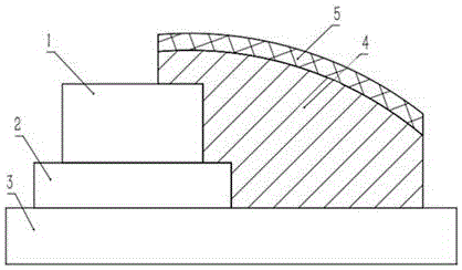
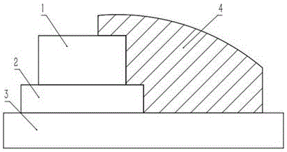
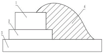
[0027] This example is mainly used to prepare air bridges on low electrode steps (such as figure 1 As shown, the sum of "1" and "2" steps is less than 4um), using a single layer of LOR photoresist as the sacrificial layer, the specific preparation process is as follows:

[0028] (1) On the substrate where the electrode steps have been etched (such as figure 1 As shown, the sum of "1" and "2" steps is less than 4um) Spin-coat a layer of LOR20A photoresist as a sacrificial layer;

[0029] (2) Spin-coat a layer of AZ52 series photoresist on the sacrificial layer as the mask layer of the sacrificial layer. After exposure and development, the pattern structure of the photoresist mask is transferred to the photoresist film to form the The required sacrificial layer graph structure ( figure 1 shown);

[0030] (3) Perform flood exposure on the substrate (exposure without photolithography mask), develop in the developer for 50s, remove the upper AZ52 series photoresist, leaving only...

Embodiment 2

[0036] This example is mainly applied to the preparation of air bridges on higher electrode steps (such as figure 1 As shown, the "1" and "2" steps add up to more than 4um), using 2 layers of LOR photoresist as the sacrificial layer, the specific preparation process is as follows:

[0037] (1) On the substrate where the electrode steps have been etched (such as figure 1 As shown, the "1" and "2" steps add up to more than 4um) and then spin-coat 2 layers of LOR20A photoresist as a sacrificial layer;

[0038] (2) Spin-coat a layer of AZ52 series photoresist on the sacrificial layer as the mask layer of the sacrificial layer. After exposure and development, the pattern structure of the photoresist mask is transferred to the photoresist film to form the The required sacrificial layer graph structure ( figure 1 shown);

[0039] (3) Perform flood exposure on the substrate (exposure without photolithography mask), develop in the developer for 50s, remove the upper AZ52 series phot...


PUM


Abstract

The invention discloses a manufacturing method of a semiconductor process air bridge. The manufacturing method has the advantages that a sacrificial layer and back electrode patterns are manufacturing by LOR-series photoresist and AZ52-series photoresist, different types LOR photoresist and different photoresist smearing rotation speeds can be selected according to the different heights of steps, and single-layer and double-layer photoresist smearing can be used flexibly; due to the fact that the LOR-series photoresist is a non-photosensitive material and the AZ52-series photoresist is a photosensitive material, a line width structure is decided by the upper-layer AZ52-series photoresist, and the high-resolution and high-photosensitivity upper-layer AZ52-series photoresist can be applied to the high-step and small-line-width device structure.

Description

technical field [0001] The invention relates to the technical field of air bridge preparation, in particular to a method for manufacturing an air bridge in a semiconductor process. Background technique [0002] In high-frequency and ultra-high-frequency devices, it is necessary to reduce the parasitic capacitance of metal electrode leads to improve the sensitivity of the device. Since the dielectric constant value of air is close to 1, using the air bridge method to realize metal electrode leads can greatly reduce parasitic capacitance, avoiding the process of depositing expensive low-permittivity dielectric film materials; at the same time, the air bridge structure provides electrode leads Low thermal resistance connections and cooling channels. [0003] At present, the existing technology generally uses positive photoresists such as AZ series and S18 series as the sacrificial layer of the air bridge process, or evaporates a metal layer on the sacrificial layer as a seed l...

Claims


Application Information

Patent Timeline
Patent Type & Authority Applications(China)
IPC IPC(8): H01L21/60G03F7/00
CPCG03F7/0035H01L24/85H01L2224/85002
Inventor 王扬华
Owner 无锡费曼科技有限公司
Why Eureka
Try Eureka