An inductively coupled plasma processing device

A technology of inductive coupling and processing devices, applied in the direction of plasma, electrical components, etc., can solve the problems of uneven distribution of plasma, low utilization rate of air flow, uneven distribution of reaction speed, etc.

Active Publication Date: 2019-05-17
ADVANCED MICRO FAB EQUIP INC CHINA
View PDF10 Cites 0 Cited by
  • Summary
  • Abstract
  • Description
  • Claims
  • Application Information

AI Technical Summary

Problems solved by technology

With this cooling structure, because the fans are placed symmetrically, the temperature distribution on the insulating material window can be symmetrical. However, because the airflows generated by the two opposite fans oppose each other, this will cause a large amount of airflow to form an upward vortex before reaching the insulating window. The utilization rate of the airflow is very low, and the middle area of ​​the insulating material window 6 has only a small amount of airflow to flow through the middle area due to the airflow hedging, so that the uneven temperature of the entire insulating material window surface still cannot be solved
[0004] If in order to obtain a uniform temperature of the insulating material window, the fan is set above the middle area of ​​the insulating material window, and the airflow is blown downward, then the traditional matching device with a large volume cannot be installed in the middle, which will cause uneven distribution of plasma below, It will also bring about the uneven distribution of the reaction velocity below.

Method used


Image

  • An inductively coupled plasma processing device
  • An inductively coupled plasma processing device
  • An inductively coupled plasma processing device

Examples


Embodiment Construction

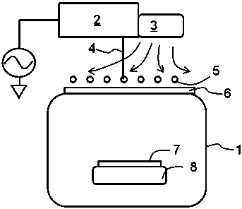
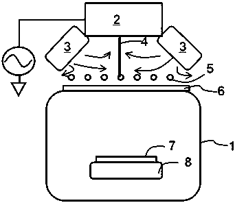
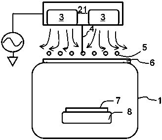
[0016] Such as image 3 Shown is a schematic diagram of the structure of the inductively coupled plasma processing device of the present invention. figure 1 Compared with the similar structure of the plasma processing device in the prior art shown, the main difference is that the matching device 21 provided above the reaction chamber 1 of the present invention is optimized in design. The traditional matching device includes a shell, which is usually made of Made of metal, the shell is separated into two parts by a shielding plate, the first part is the DC area, and the second part is the radio frequency area. The second part includes components such as inductors, capacitors, variable capacitors, and resistors that pass radio frequency currents. The first part includes DC power supplies output regulated DC power. The motor is used to drive the variable capacitors in the radio frequency area. It can also include a controller for Control the operation of each device in the entire m...


PUM


Abstract

An inductive coupling plasma processing apparatus comprises a reaction chamber and a matcher. An insulating material window is located on a reaction chamber top. A pedestal is located at a lower portion in the reaction chamber and is used for fixing a substrate. At least one substrate is arranged on the pedestal. An inductance coil is arranged above the insulating material window. The inductance coil comprises a radio frequency energy input terminal which is located at an upper portion of an insulating material window center area. The matcher comprises one shell. The shell comprises a radio frequency input terminal connected to a radio frequency power supply and a radio frequency output terminal located at a shell bottom center. The radio frequency output terminal is downwardly extended through a radio frequency lead and is connected to the radio frequency input terminal of the inductance coil. A shell bottom comprises a plurality of openings which surround the radio frequency output terminal. Fans, which are installed in the openings, blow an air flow downwardly to the insulating material window.

Description

Technical field [0001] The invention relates to the technical field of semiconductor manufacturing, in particular to the structural design of an inductively coupled plasma processor. Background technique [0002] Such as figure 1 As shown, the conventional inductive coupling (ICP) plasma processing apparatus includes a reaction chamber 1, a susceptor 8 is included in the reaction chamber, and a lower electrode is included in the susceptor. The wafer 7 to be processed is included above the susceptor. A radio frequency power supply outputs radio frequency power through the output end of a matcher 2, and the output end of the matcher 2 is connected to the inductance coil below through a wire 4. The inductor coil 5 is located above the top of the reaction chamber at the same time, and the inductor coil 5 feeds the radio frequency electromagnetic field into the space of the reaction chamber through the insulating material window 6 located on the top of the reaction chamber 1 to gener...

Claims


Application Information

Patent Timeline
Patent Type & Authority Patents(China)
IPC IPC(8): H05H1/46
Inventor 倪图强左涛涛吴狄
Owner ADVANCED MICRO FAB EQUIP INC CHINA
Why Eureka
Try Eureka