Signal transmission insulative device and power semiconductor module

A power semiconductor and signal transmission technology, which is applied in the direction of semiconductor devices, semiconductor/solid-state device manufacturing, semiconductor/solid-state device components, etc., can solve problems such as insulation damage, achieve the effect of improving insulation withstand voltage and suppressing the reduction of transmission characteristics

Active Publication Date: 2017-05-24
MITSUBISHI ELECTRIC CORP
View PDF7 Cites 3 Cited by
  • Summary
  • Abstract
  • Description
  • Claims
  • Application Information

AI Technical Summary

Problems solved by technology

In addition, there are many corners in the signal transmission insulation device having a transformer structure, and when the applied voltage increases, insulation breakdown occurs from any corner of the upper coil or the lower coil

Method used


Image

  • Signal transmission insulative device and power semiconductor module
  • Signal transmission insulative device and power semiconductor module
  • Signal transmission insulative device and power semiconductor module

Examples


Embodiment approach 1

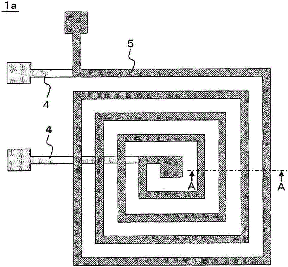
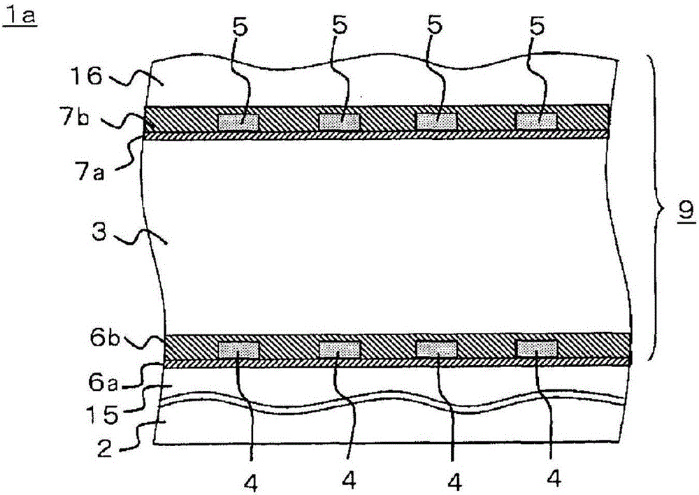
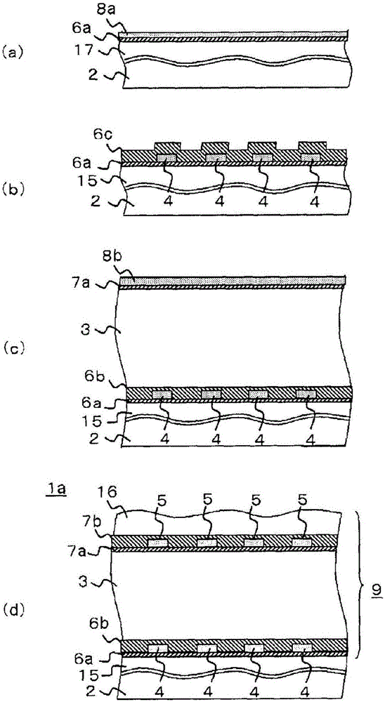
[0032] First, the configuration of the signal transmission insulating device according to Embodiment 1 of the present invention will be described. figure 1 It is a plan view showing the structure of the signal transmission insulating device 1a according to Embodiment 1 of the present invention. figure 2 It is a sectional view showing the structure of the signal transmission insulating device 1a according to Embodiment 1 of the present invention. also, figure 2 equivalent to figure 1 A-A sectional view in .

[0033] exist figure 1 Among them, the signal transmission insulating device 1 a includes a coil-shaped first coil 4 and a second coil 5 formed by winding wiring multiple turns, and the first coil 4 and the second coil 5 face each other to form a transformer. In addition, in figure 1 In FIG. 2 , the portion of the first coil 4 that overlaps the second coil 5 is omitted from illustration.

[0034] exist figure 2 Among them, the signal transmission insulating device...

Embodiment approach 2

[0066] The structure of this invention is not limited to the structure of the signal transmission insulating device 1a of Embodiment 1, It can also be set as another structure. In particular, when the semiconductor substrate 2 is conductive and the first coil 4 and the semiconductor substrate 2 are grounded, the generation of electric field concentration at the corner of the first coil 4 facing the semiconductor substrate 2 can be suppressed, so it is possible to omit the installation of The structure of the second insulating film 6a on the lower side of the first coil 4 can reduce the number of manufacturing steps and reduce the production cost. Therefore, the structure different from the signal transmission insulating device 1a of Embodiment 1 is demonstrated. In addition, the part of the second insulating film that is different from Embodiment 1 of the present invention will be described below, and the description of other parts that are the same or correspond to each other...

Embodiment approach 3

[0081] The structure of the signal transmission insulation device 1c of Embodiment 3 is demonstrated. Figure 8 It is a cross-sectional view showing the structure of a signal transmission insulating device 1c according to Embodiment 3 of the present invention. exist Figure 8 in, with figure 2 Parts with the same symbols represent the same or corresponding structures. In addition, this embodiment differs from Embodiment 1 in the structure of the second insulating films 6 a , 6 b , and the third insulating films 7 a , 7 b, so only the differences will be described below, and descriptions of other structures will be omitted.

[0082] exist Figure 8 In the signal transmission insulating device 1c of Embodiment 3, a dielectric having a higher permittivity than the dielectric used as the first insulating film 3 is used as the second insulating films 6a, 6b and the third insulating films 7a, 7b. For example, when using SiO 2 When the film is used as the first insulating film ...


PUM


Abstract

A signal transmission insulative device is provided with: a first coil; a second coil facing the first coil and forming a transformer with the first coil; a first insulation film comprising a first dielectric body in the space where the first coil and the second coil face one another; a second insulation film surrounding the first coil and comprising a second dielectric body that has a resistivity lower than the first dielectric body; and a third insulation film surrounding the second coil and comprising a third dielectric body that has a resistivity lower than the first dielectric body. Or, the signal transmission insulative device is provided with: a first coil; a second coil facing the first coil and forming a transformer with the first coil; a first insulation film comprising a first dielectric body in the space where the first coil and the second coil face one another; a second insulation film surrounding the first coil and comprising a second dielectric body that has a dielectric constant higher than the first dielectric body; and a third insulation film surrounding the second coil and comprising a third dielectric body that has a dielectric constant higher than the first dielectric body.

Description

technical field [0001] The present invention relates to a signal transmission insulating device and a power semiconductor module provided with the signal transmission insulating device. Background technique [0002] As a conventional signal transmission insulation device having a thin-film transformer structure, there is known a device in which a lower coil is formed at the bottom of a recess provided on a semiconductor substrate, and the recess is filled with liquid polyimide resin and cured, Accordingly, a first insulating film is formed, and an upper coil is formed thereon. The thickness of the first insulating film is adjusted to ensure a dielectric breakdown voltage between the lower coil and the upper coil (see, for example, Patent Document 1). [0003] In such a signal transmission insulating device having a thin-film transformer structure, when a voltage is applied to the upper coil and the lower coil, electric field concentration occurs at respective corners of the ...

Claims


Application Information

Patent Timeline
Patent Type & Authority Applications(China)
IPC IPC(8): H01L21/822H01F17/00H01F19/00H01F27/32H01L27/04
CPCH01F27/32H01F27/2804H01L23/62H01L23/645H01L25/18H01F2027/2809G11C11/34H01L23/3738H01L24/03H01L25/162H04L1/0006H05K7/1432
Inventor 菅健一钓本崇夫盐田裕基诸熊健一折田昭一为谷典孝井上贵公鱼田紫织
Owner MITSUBISHI ELECTRIC CORP
Why Eureka
Try Eureka