
Switching circuits having ferrite beads

A ferrite bead and circuit technology, applied in circuits, electronic switches, transistors, etc., can solve the problems of stable interference and effective switching functions

Active Publication Date: 2017-05-24
TRANSPHORM INC
View PDF5 Cites 9 Cited by
  • Summary
  • Abstract
  • Description
  • Claims
  • Application Information

AI Technical Summary

Problems solved by technology

If a half-bridge is implemented using a conventional package, the unwanted inductance introduced by the package leads can cause significant ringing and oscillations related to the transistor current flowing through the circuit, which can interfere with stable, efficient switching function

Method used


Image

  • Switching circuits having ferrite beads
  • Switching circuits having ferrite beads
  • Switching circuits having ferrite beads

Examples


Embodiment Construction

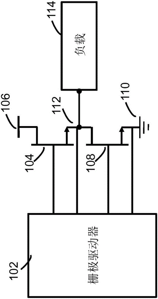
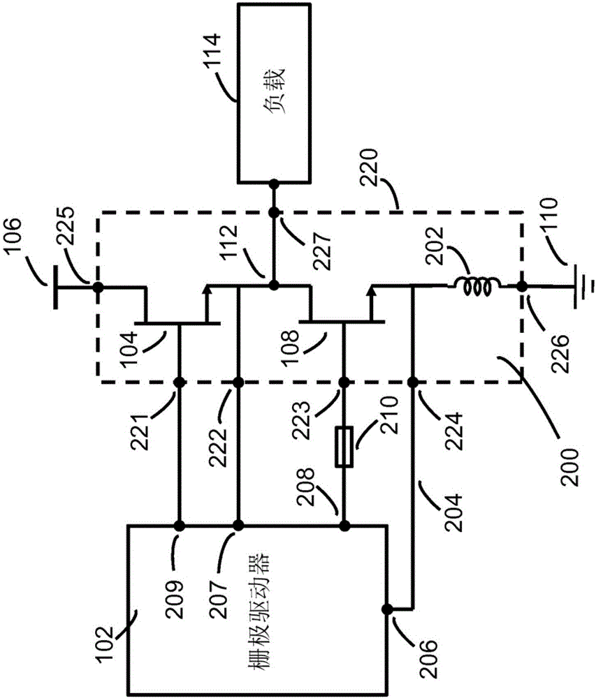
[0037] figure 2 is a circuit diagram of an example switching circuit, a portion of which is implemented as an electronic module 200 . Module 200 includes a high-side switch 104 connected in series with a low-side switch 108 in a half-bridge configuration. The module enclosure indicated by dashed line 220 includes nodes 221-227. Nodes 221 and 222 are coupled (eg, electrically connected) to the gate and source of switch 104 , respectively. Nodes 223 and 224 are coupled (eg, electrically connected) to the gate and source of switch 108 , respectively. Node 225 is coupled (eg, electrically connected) to the drain of switch 104 . Node 226 is coupled (eg, electrically connected) to the source of switch 108 through a connection having parasitic inductance 202 . Output node 227 is coupled (eg, electrically connected) to load node 112 at the output of the half-bridge formed by switches 104 and 108 . The circuit also includes a gate driver 102 connected to the nodes 221-224 of the m...


PUM


Abstract

A circuit includes an electronic component package that comprises at least a first lead, a III-N device in the electronic component package, a gate driver, and a ferrite bead. The III-N device comprises a drain, gate, and source, where the source is coupled to the first lead. The gate driver comprises a first terminal and a second terminal, where the first terminal is coupled to the first lead. The ferrite bead is coupled between the gate of the III-N transistor and the second terminal of the gate driver. When switching, the deleterious effects of the parasitic inductance of the circuit gate loop are mitigated by the ferrite bead.

Description

technical field [0001] This application relates to the use of ferrite beads to stabilize switching circuits such as high speed III-N power switches. Background technique [0002] Using high-speed III-N power switches involves balancing the requirements for heat transfer, ease of assembly, and high-speed, low-inductance electrical interconnects. Conventional leaded power packages (any of the variations such as the TO-220 package) can be used with III-N power switches. The combination of metal mounting tabs and flexible copper leads allows the package to be attached to an effective heat sink in various configurations. Utilizing conventional soldering techniques to connect to the PCB allows for ease of manufacture. [0003] However, package leads often introduce undesirable inductance. The reduced switching speed caused by this inductance can be an acceptable design hazard, but instability can still cause problems. Since a power switch can be a high gain device, if allowed ...

Claims


Application Information

Patent Timeline
Patent Type & Authority Applications(China)
IPC IPC(8): H01L23/50H01L21/82
CPCH01L2224/48091H01L2224/48247H03K17/102H03K17/122H03K17/165H03K2017/6875H01L2224/48137H01L2924/00014H01L2924/13055H03K17/16H01L29/2003H03K17/162H01L2924/13091H01L2224/45099H01L2924/00H01L29/16H01L23/49562H01L23/552H01L23/645H01L24/48H01L27/0605H01L27/0883H01L2224/48106H01L2924/3025H03K17/04106
Inventor 王展吴毅锋詹姆斯·哈尼
Owner TRANSPHORM INC
Learn More