Touch screen, manufacturing method thereof and display apparatus

A manufacturing method and touch screen technology, applied in organic semiconductor devices, photovoltaic power generation, instruments, etc., can solve problems such as unfavorable light and thin design, and achieve the effects of low power consumption, low working voltage, and low surface design

Pending Publication Date: 2017-05-31
BOE TECH GRP CO LTD +1
View PDF6 Cites 14 Cited by
  • Summary
  • Abstract
  • Description
  • Claims
  • Application Information

AI Technical Summary

Problems solved by technology

[0003] In view of this, the embodiments of the present invention provide a touch screen, its manufacturing method and a

Method used


Image

  • Touch screen, manufacturing method thereof and display apparatus
  • Touch screen, manufacturing method thereof and display apparatus
  • Touch screen, manufacturing method thereof and display apparatus

Examples


Embodiment Construction

[0035] The specific implementations of the touch screen, its manufacturing method, and the display device provided by the embodiments of the present invention will be described in detail below with reference to the accompanying drawings.

[0036] The thickness and shape of each film layer in the drawings do not reflect the true ratio, and the purpose is only to illustrate the content of the present invention schematically.

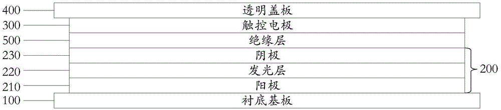
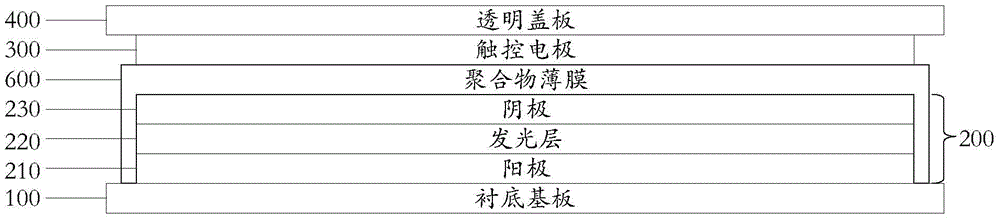
[0037] An embodiment of the present invention provides a touch screen, such as Figure 2a with Figure 2b As shown, it includes: a base substrate 100, a plurality of electroluminescent pixel units 200 arranged in an array arranged on the base substrate 100, and further includes: touch electrodes 300 arranged in an array; and touch electrodes 300 are arranged It is above the electroluminescence pixel unit 200 and insulated from the electroluminescence pixel unit 200.

[0038] In the above-mentioned touch screen provided by the embodiment of the present invention, ...


PUM


Abstract

The invention discloses a touch screen, a manufacturing method thereof and a display apparatus. According to the invention, touch electrodes in arrayed arrangement are arranged in an OLED display panel, and more particularly, the touch electrodes are arranged on electroluminescent pixel units which are insulated from each other. In this way, the thickness of a touch screen display apparatus can be reduced, which facilitates the thinned design of a product.

Description

Technical field [0001] The present invention relates to the technical field of touch display, in particular to a touch screen, a manufacturing method thereof and a display device. Background technique [0002] Organic light-emitting diodes (OLED) is a display device encapsulated by organic materials. It has the advantages of low working voltage, fast response speed, high luminous efficiency, wide viewing angle and wide working temperature. It is conducive to the thinness, low power consumption and curved surface design of the display device. At present, most of the existing OLED-based touch products adopt such figure 1 The plug-in touch structure shown is to make OLED display panel 01 and touch panel 02 respectively, and glue the two panels together to form a complete touch display device. This structure will increase the overall thickness of the OLED device , Is not conducive to the thin and light design of the product. Summary of the invention [0003] In view of this, the emb...

Claims


Application Information

Patent Timeline
IPC IPC(8): H01L27/32G06F3/041
CPCG06F3/041H10K59/00G06F3/0412G06F2203/04112G06F3/0443Y02E10/549G06F3/04164G06F3/0448H10K59/40H10K50/822H10K50/844G06F3/044H10K71/00H10K77/111H10K2102/311G06F2203/04102G06F2203/04103
Inventor 刘伟董学陈小川王海生丁小梁杨盛际刘英明赵卫杰刘红娟李昌峰王鹏鹏薛海林
Owner BOE TECH GRP CO LTD
Why Eureka
Try Eureka