Source electrode follower buffer circuit

A source follower and buffer circuit technology, applied in electrical components, physical parameter compensation/prevention, code conversion, etc., can solve the problems of weakened even-order harmonic suppression and poor linearity, and reduce signal distortion. , the effect of eliminating signal errors

Active Publication Date: 2017-05-31
UNIV OF ELECTRONICS SCI & TECH OF CHINA
View PDF1 Cites 10 Cited by
  • Summary
  • Abstract
  • Description
  • Claims
  • Application Information

AI Technical Summary

Problems solved by technology

The disadvantage is that when the input signal amplitude is large, the input tube will enter the linear region, making the linearity worse; at the same time, the structure is a pseudo-differential structure, which weakens the ability to suppress even-order harmonics when the circuit is implemented

Method used


Image

  • Source electrode follower buffer circuit
  • Source electrode follower buffer circuit
  • Source electrode follower buffer circuit

Examples


Embodiment Construction

[0009] The present invention is described in detail below in conjunction with accompanying drawing:

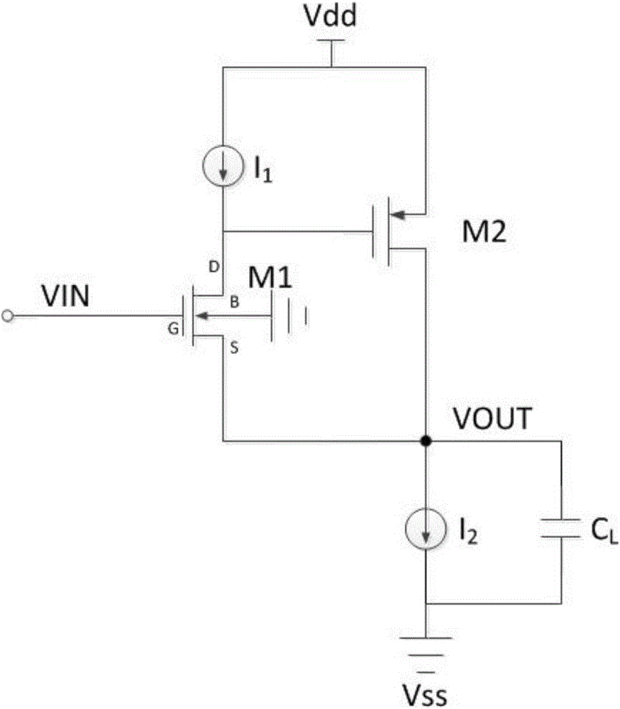
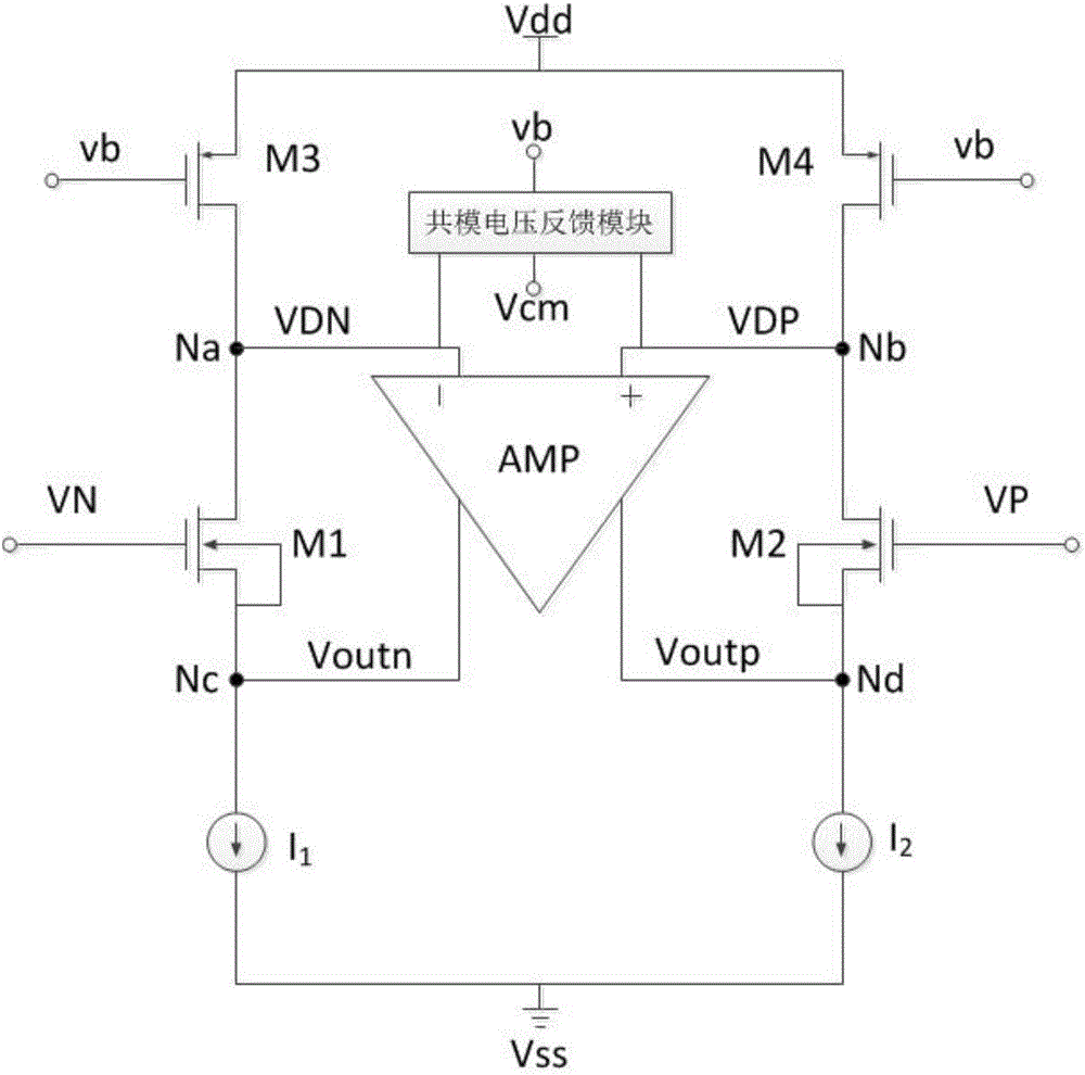
[0010] Such as figure 2 As shown, a source follower buffer circuit of the present invention is used for the input end of the analog-to-digital converter, and includes a first NMOS transistor M1, a second NMOS transistor M2, a first PMOS transistor M3, and a second PMOS transistor. Tube M4, the first current source I1, the second current source I2, a fully differential operational amplifier and a common-mode voltage feedback module; the source of the first PMOS transistor M3 is connected to the power supply, and its gate is connected to the output of the common-mode voltage feedback module Feedback signal; the source of the second PMOS transistor M4 is connected to the power supply, and its gate is connected to the feedback signal output by the common-mode voltage feedback module; the drain of the first NMOS transistor M1 is connected to the drain of the first PMOS transistor ...


PUM


Abstract

The invention belongs to the technical field of analog-digital converter, and in particular relates to a source electrode follower buffer circuit. The circuit comprises a first NMOS transistor M1, a second NMOS transistor M2, a first PMOS transistor M3, a second PMOS transistor M4, a first current source I1, a second current source I2, a fully differential operational amplifier and a common-mode voltage feedback module, wherein the M1, M2, M3 and M4 always work in a saturation area, source electrode voltages of the M1 and M2 follow the change of VN and VP, an input pair transistor substrate is in short circuit with the source electrode and thus the bulk effect of the transistors is eliminated, a feedback loop formed by the fully differential operational amplifier under a large-swing input signal provides stable static working points for the M1 and M2, when a load is connected with the output end, the feedback loop help the transistors M1 and M2 charge and discharge, current change of the transistors M1 and M2 is reduced, and the linearity of the follower is improved. According to the circuit provided by the invention, the bulk effect and the channel length modulation effect are avoided, current change in the transistor in the follower is greatly reduced, and the circuit has the advantage of high linearity.

Description

technical field [0001] The invention belongs to the technical field of analog-to-digital converters, and in particular relates to a source follower buffer circuit. Background technique [0002] The buffer based on the source-follower structure is used as the input terminal of the analog-to-digital converter, which is one of the most important modules of the analog-to-digital converter, which directly determines the accuracy of the analog-to-digital converter, and usually requires high linearity for the input signal . [0003] A conventional source follower such as figure 1 shown. The disadvantage is that when the input signal amplitude is large, the input tube will enter the linear region, making the linearity worse; at the same time, the structure is a pseudo-differential structure, which weakens the ability to suppress even harmonics when the circuit is implemented. Contents of the invention [0004] The object of the present invention is to propose a source follower ...

Claims


Application Information

Patent Timeline
Patent Type & Authority Applications(China)
IPC IPC(8): H03M1/06
CPCH03M1/0636
Inventor 李靖王明辉胡远冰宁宁
Owner UNIV OF ELECTRONICS SCI & TECH OF CHINA
Why Eureka
Try Eureka