Sticky chip detection method and system, reaction chamber and semiconductor processing equipment

A detection system and detection method technology, applied in semiconductor/solid-state device manufacturing, electrical components, circuits, etc., can solve problems such as difficulty in releasing electrostatic charges, breakage of lifting pins, tilting of substrates, etc., and achieve the goal of improving reliability and safety Effect

Active Publication Date: 2019-05-31
BEIJING NAURA MICROELECTRONICS EQUIP CO LTD
View PDF4 Cites 0 Cited by
  • Summary
  • Abstract
  • Description
  • Claims
  • Application Information

AI Technical Summary

Problems solved by technology

[0004] In practical application, it is found that for the substrate S of semiconductor material or insulating material, there are certain difficulties in the discharge of electrostatic charges, that is, there may be residual charges, and the adsorption effect caused by the residual charges will cause the substrate to stick. The sticking phenomenon is not serious. At this time, the rise of the lifting needle will cause the substrate to tilt, such as figure 2 As shown, if the manipulator takes the film at this time, the mechanical arm will be damaged and the substrate S will be smashed; if the film sticking phenomenon is serious, the lifting needle 11 will even break when it rises

Method used


Image

  • Sticky chip detection method and system, reaction chamber and semiconductor processing equipment
  • Sticky chip detection method and system, reaction chamber and semiconductor processing equipment
  • Sticky chip detection method and system, reaction chamber and semiconductor processing equipment

Examples


Embodiment Construction

[0032] In order for those skilled in the art to better understand the technical solutions of the present invention, the method and system for detecting sticky chips, the reaction chamber and the semiconductor processing equipment provided by the present invention will be described in detail below with reference to the accompanying drawings.

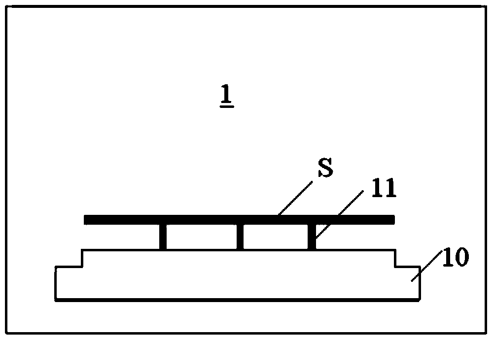
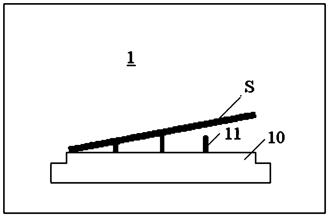
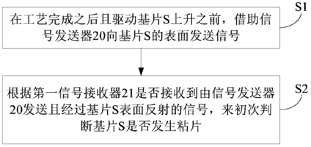
[0033] image 3 It is a flow chart of the method for detecting sticky film provided by the first embodiment of the present invention. Figure 4 for adoption image 3 A schematic diagram of the detection principle of the sticking detection method shown when the substrate does not stick. Figure 5 for adoption image 3 The schematic diagram of the detection principle of the sticking detection method shown when the sticking occurs on the entire lower surface of the substrate. Please also refer to Figure 3 ~ Figure 5 , the sticky sheet detection method comprises the following steps:

[0034] S1, after the process is completed and before t...


PUM


Abstract

The invention provides a substrate bonding detection method and a substrate bonding detection system. The substrate bonding detection method comprises the steps of: transmitting a signal to the surface of a substrate by means of a signal transmitter after the completion of process and before the substrate is driven to ascend; and preliminarily judging whether substrate bonding occurs according to whether a signal receiver receives the signal which is transmitted by the signal transmitter and reflected through the surface of the substrate. According to the substrate bonding detection method and the substrate bonding detection system provided by the invention, whether the substrate bonding occurs is judged after the completion of process and before the substrate is driven to ascend, thus, the substrate bonding problem can be discovered as early as possible during the substrate unloading process, thereby being capable of improving a series of problems caused by substrate bonding later as early as possible, such as the problems that lifting pins are prone to fracture when jacking up the substrate, a mechanical arm is damaged and even the substrate is crashed when the substrate is fetched by the mechanical arm after being jacked up.

Description

technical field [0001] The invention belongs to the technical field of semiconductor processing, and in particular relates to a method and system for detecting sticky chips, a reaction chamber and semiconductor processing equipment. Background technique [0002] For semiconductor processing equipment such as plasma etching equipment, physical vapor deposition equipment, and chemical vapor deposition equipment, electrostatic chucks are often used to fix the substrate in the chamber, and at the same time, the cooling function of the electrostatic chuck itself is used to cool the substrate. The temperature of the substrate is also controlled by blowing heat exchange gas to the back of the substrate through the electrostatic chuck to meet the process requirements. [0003] figure 1 For a schematic diagram of the existing reaction chamber, see figure 1 , the reaction chamber is provided with an electrostatic chuck 10 and a plurality of lifting pins 11, both of which are used to...

Claims


Application Information

Patent Timeline
Patent Type & Authority Patents(China)
IPC IPC(8): H01L21/60H01L21/67
Inventor 刘云波
Owner BEIJING NAURA MICROELECTRONICS EQUIP CO LTD
Why Eureka
Try Eureka