Semiconductor processing apparatus
A processing equipment and semiconductor technology, applied in semiconductor/solid-state device manufacturing, discharge tubes, electrical components, etc., can solve problems such as etching defects, particle drop, and affecting product yield, so as to avoid etching defects and improve product quality. The effect of yield
- Summary
- Abstract
- Description
- Claims
- Application Information
AI Technical Summary
Problems solved by technology
Method used
Image

Examples
Embodiment Construction
[0021] In order for those skilled in the art to better understand the technical solutions of the present invention, the semiconductor processing equipment provided by the present invention will be described in detail below in conjunction with the accompanying drawings.
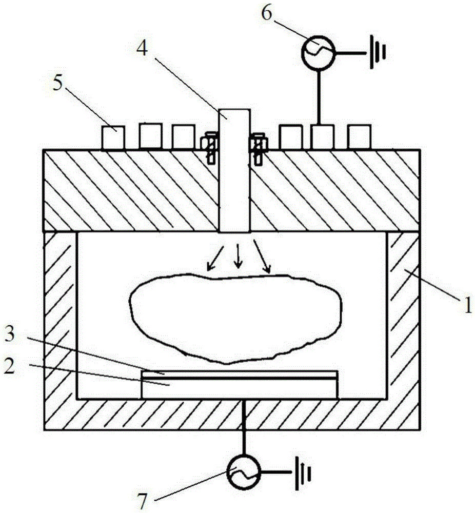
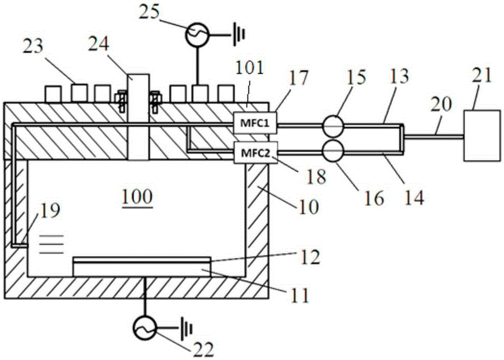
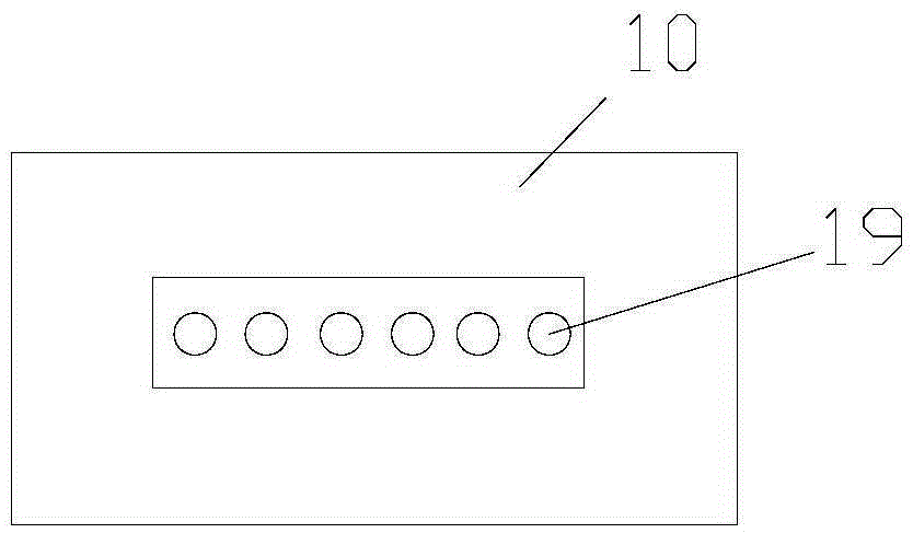
[0022] figure 2 A cross-sectional view of the semiconductor processing equipment provided by the embodiment of the present invention. see figure 2 , the semiconductor processing equipment includes a reaction chamber 100 , a process gas path and a purging device, wherein a carrying device 11 for fixing a wafer 12 is provided inside the reaction chamber 100 , and is electrically connected to a bias power supply 22 . The carrying device 11 can be an electrostatic chuck or a mechanical chuck or the like. Moreover, a coil 23 is provided above the top dielectric window 101 of the reaction chamber 100 , and is electrically connected to an excitation power source 25 . Moreover, a central nozzle 24 is provided on ...
PUM
 Abstract
Description
Claims
Application Information
 - Generate Ideas
- Intellectual Property
- Life Sciences
- Materials
- Tech Scout
- Unparalleled Data Quality
- Higher Quality Content
- 60% Fewer Hallucinations
Browse by: Latest US Patents, China's latest patents, Technical Efficacy Thesaurus, Application Domain, Technology Topic, Popular Technical Reports.
© 2025 PatSnap. All rights reserved.Legal|Privacy policy|Modern Slavery Act Transparency Statement|Sitemap|About US| Contact US: help@patsnap.com