Semiconductor structure and manufacturing method thereof

A manufacturing method and semiconductor technology, which are applied in the fields of semiconductor/solid-state device manufacturing, semiconductor devices, and semiconductor/solid-state device components, etc., can solve the problems of difficulty in the capacitance value of a single capacitor, increase the structure of a single capacitor, and high leakage current, and avoid problems such as Etching defects, avoidance of tipping or collapse, effect of large capacitance values

Pending Publication Date: 2022-03-15
CHANGXIN MEMORY TECH INC
View PDF0 Cites 0 Cited by
  • Summary
  • Abstract
  • Description
  • Claims
  • Application Information

AI Technical Summary

Problems solved by technology

[0002] Increasing the capacitance of a single capacitive structure or maintaining the capacitance of a single capacitor becomes increasingly difficult as the dimensions of semiconductor structures shrink
When using the same dielectric

Method used


Image

  • Semiconductor structure and manufacturing method thereof
  • Semiconductor structure and manufacturing method thereof
  • Semiconductor structure and manufacturing method thereof

Examples


Embodiment Construction

[0030] In order to make the purpose, technical solutions and advantages of the embodiments of the present invention clearer, the embodiments of the present invention will be described in detail below with reference to the accompanying drawings. However, those skilled in the art can understand that in each embodiment of the present invention, many technical details are provided for readers to better understand the present application. However, even without these technical details and various changes and modifications based on the following embodiments, the technical solutions claimed in this application can also be realized.

[0031] Figure 1 to Figure 23 A schematic diagram of a cross-sectional structure corresponding to each step of a method for fabricating a semiconductor structure provided by an embodiment of the present invention.

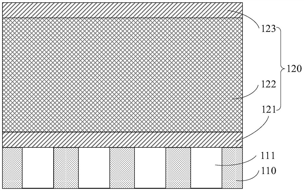
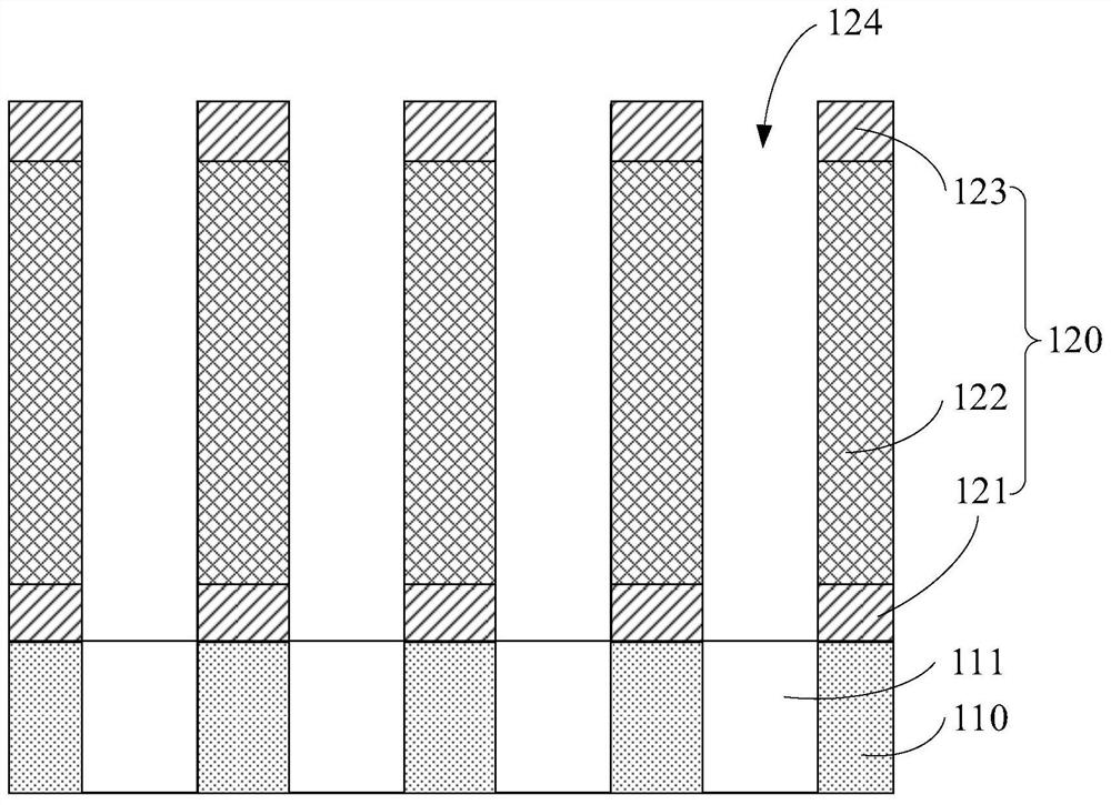
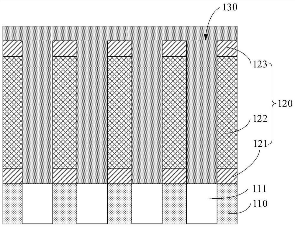
[0032] refer to figure 1 , providing a substrate 110 with a conductive structure 111 inside; forming a first dielectric layer 120 on the su...


PUM


Abstract

The embodiment of the invention provides a semiconductor structure and a manufacturing method thereof, and the semiconductor structure comprises a substrate which is internally provided with a conductive structure; the first lower electrode and the second lower electrode are sequentially stacked, the first lower electrode is located between the second lower electrode and the substrate, the first lower electrode is columnar, the second lower electrode is groove-shaped, and the first lower electrode is electrically connected with the conductive structure; the first dielectric layer covers the surface of the side wall of the first lower electrode, and the first upper electrode is located on the side, away from the first lower electrode, of the first dielectric layer; and a second dielectric layer and a second upper electrode, the second dielectric layer covers the inner wall and the bottom surface of the second lower electrode, and the second upper electrode is filled in the groove of the second lower electrode. The invention provides a novel capacitor structure which is favorable for improving the capacitance value of a single capacitor structure.

Description

technical field [0001] Embodiments of the present invention relate to the field of semiconductors, and in particular to a semiconductor structure and a manufacturing method thereof. Background technique [0002] As semiconductor structures shrink in size, it becomes increasingly difficult to increase the capacitance of a single capacitive structure or maintain the capacitance of a single capacitor. When using the same dielectric layer material, the increase in capacitance can only be achieved by increasing the surface area of ​​the electrode plate or reducing the thickness of the dielectric layer, but the latter may cause problems with excessive leakage current. [0003] Therefore, changing the capacitor structure to increase the surface area of ​​the electrode plate is an important development direction for increasing the capacitance value of the capacitor structure. Contents of the invention [0004] Embodiments of the present invention provide a semiconductor structure...

Claims


Application Information

Patent Timeline
IPC IPC(8): H01L23/522H01L21/768H01L27/108H01L21/8242
CPCH01L23/5222H01L21/768H10B12/30H10B12/03H01L23/522H10B12/00
Inventor 朱柄宇洪海涵余崟魁
Owner CHANGXIN MEMORY TECH INC
Why Eureka
Try Eureka