Production method of metal gate device

A metal gate and device technology, applied in the field of metal gate device preparation, can solve problems such as reliability failure, MOS device failure, device characteristic degradation, etc., to ensure continuity, avoid damage, and improve device performance and reliability.

Pending Publication Date: 2021-03-26
上海微阱电子科技有限公司
View PDF0 Cites 0 Cited by
  • Summary
  • Abstract
  • Description
  • Claims
  • Application Information

AI Technical Summary

Problems solved by technology

[0005] The formation process of the conventional metal gate includes the process steps of dummy gate layer deposition, removal and metal gate formation. The dummy gate layer needs to be removed before the metal gate is prepared. Etching, wet etching, or a combination of dry and wet methods, but these three methods have their own shortcomings in the implementation process
[0006] figure 1 This is a cross-sectional view of the dummy gate layer in the PMOS area using a dry etching process. The plasma of the dry etching causes damage to the gate oxide layer above the active region, which causes degradation of device characteristics and reliability failure
[0007] figure 2 This is a cross-sectional view of the dummy gate layer in the PMOS area using a wet etching process. Due to the isotropic characteristics of wet etching, the dummy gate layer in the NMOS area is eroded at the same time, forming an arc-shaped loss of the NMOS dummy gate layer, causing the subsequent PMOS The intrusion of the metal gate into the NMOS region causes the failure of the MOS device; at the same time, the curved sidewall of the dummy gate layer causes the discontinuity of the deposition of the subsequent metal gate barrier layer and the diffusion of metal elements, which will also cause the degradation of device characteristics and reliability failure
[0008] image 3 In order to use the dry method first, and then use the wet method to remove the cross-sectional view of the dummy gate layer in the PMOS area. This method can avoid the damage of the dry etching plasma to the gate oxide layer, but the wet method will cause the dummy gate layer. The inscribed topography of the bottom of the layer will cause the discontinuity of the deposition of the subsequent metal gate barrier layer and the diffusion of metal elements, which will eventually lead to the degradation of device characteristics and reliability failure

Method used


Image

  • Production method of metal gate device
  • Production method of metal gate device
  • Production method of metal gate device

Examples


Embodiment Construction

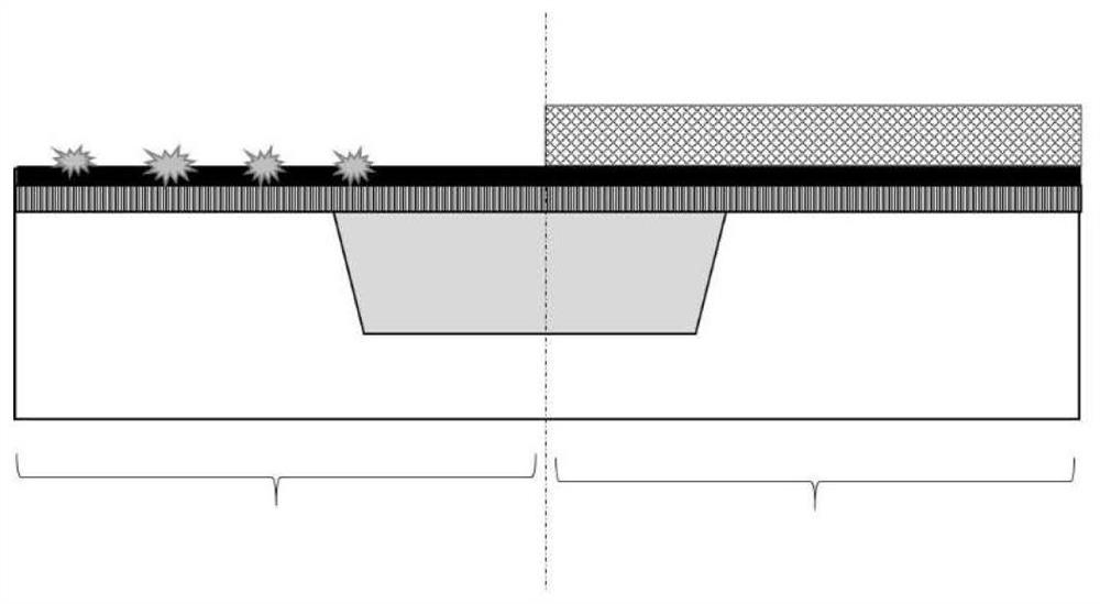
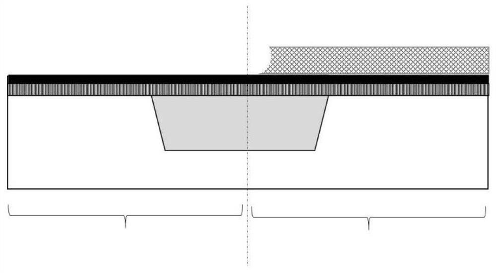
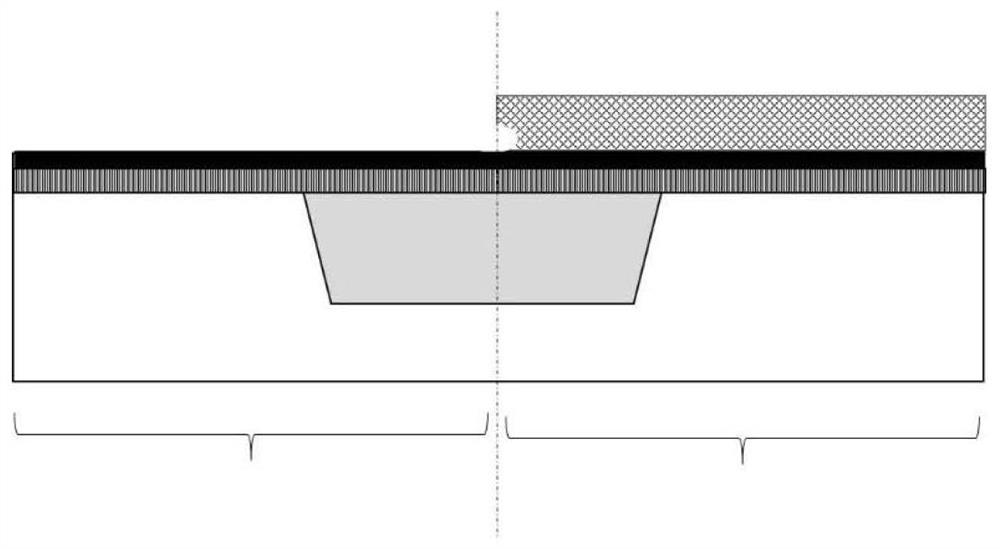
[0038] In order to make the content of the present invention clearer and easier to understand, the content of the present invention will be further described below in conjunction with the accompanying drawings. Of course, the present invention is not limited to this specific embodiment, and general replacements known to those skilled in the art are also covered within the protection scope of the present invention.

[0039] It should be noted that, in the following specific embodiments, when describing the embodiments of the present invention in detail, in order to clearly show the structure of the present invention for the convenience of description, the structures in the drawings are not drawn according to the general scale, and are drawn Partial magnification, deformation and simplification are included, therefore, it should be avoided to be interpreted as a limitation of the present invention.

[0040] In order to make the purpose, technical scheme and advantages of the pre...


PUM


Abstract

The invention provides a production method for a metal gate device. The method comprises the steps: forming a first opening in a pseudo gate layer of a second region, and enabling an extension line ofa side wall of one side of the first opening to be aligned with a connection line of the first region and the second region; forming a first sacrificial layer and a second sacrificial layer filling the first opening on the pseudo gate layer; etching the first sacrificial layer and the pseudo gate layer of the first region to form a second opening, wherein the side wall of the second opening exposes the second sacrificial layer; and forming a first gate structure in the second opening. According to the invention, the second sacrificial layer is formed at the junction of the first region and the second region, and the second sacrificial layer is used as the side wall barrier layer so that in the process of removing the pseudo gate layer of the first region by adopting a wet etching process,the etching defect of the side wall of the pseudo gate layer of the second region is avoided, and meanwhile, the damage of a dry etching process to the gate dielectric layer is also avoided; and salient significance is possessed.

Description

technical field [0001] The invention relates to the field of semiconductor manufacturing, and more particularly, to a method for preparing a metal gate device. Background technique [0002] For half a century, driven by Moore's Law, the number of transistors that can be accommodated in an integrated circuit has doubled every 18 months, and the size of transistors has also shrunk. With the continuous shrinking of the transistor feature size in CMOS circuits, the gate dielectric SiO 2 The thickness of the transistor is also constantly thinning, the insulating layer SiO in the transistor 2 Has reached the physical limit of about 10A, SiO below 2nm 2 It is no longer an ideal insulator, and there will be obvious tunneling leakage, and the leakage will increase exponentially as the thickness decreases. SiO below 1nm 2 The leakage current will be unacceptably large, so the High-K / Metal Gate (HKMG) technology is used in the high-performance process. [0003] HKMG technology refe...

Claims


Application Information

Patent Timeline
Patent Type & Authority Applications(China)
IPC IPC(8): H01L21/28H01L21/8238H01L27/092
CPCH01L21/28079H01L21/823828H01L27/0922
Inventor 顾学强
Owner 上海微阱电子科技有限公司
Why Eureka
Try Eureka