Intermediate structure of micro-LED unit and manufacturing method thereof

A technology of light-emitting diodes and manufacturing methods, applied in semiconductor/solid-state device manufacturing, electrical components, electric solid-state devices, etc., can solve the problems of difficult mass production, high production cost, labor and time consumption, etc., and achieve success rate and efficiency improvement , the effect of large contact area

Active Publication Date: 2017-06-09
AU OPTRONICS CORP
View PDF3 Cites 58 Cited by
  • Summary
  • Abstract
  • Description
  • Claims
  • Application Information

AI Technical Summary

Problems solved by technology

[0002] In the process of manufacturing the existing micro-LED intermediary structure, it is often necessary to use extremely high-precision and expensive transposition tips, which makes mass production difficult and the production cost is too high
Moreo

Method used


Image

  • Intermediate structure of micro-LED unit and manufacturing method thereof
  • Intermediate structure of micro-LED unit and manufacturing method thereof
  • Intermediate structure of micro-LED unit and manufacturing method thereof

Examples


Embodiment Construction

[0094] The present invention will be described in detail below in conjunction with the accompanying drawings and specific embodiments, but not as a limitation of the present invention.

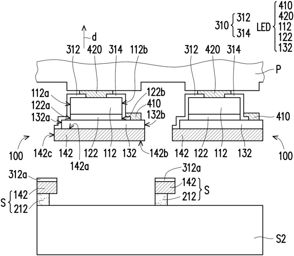
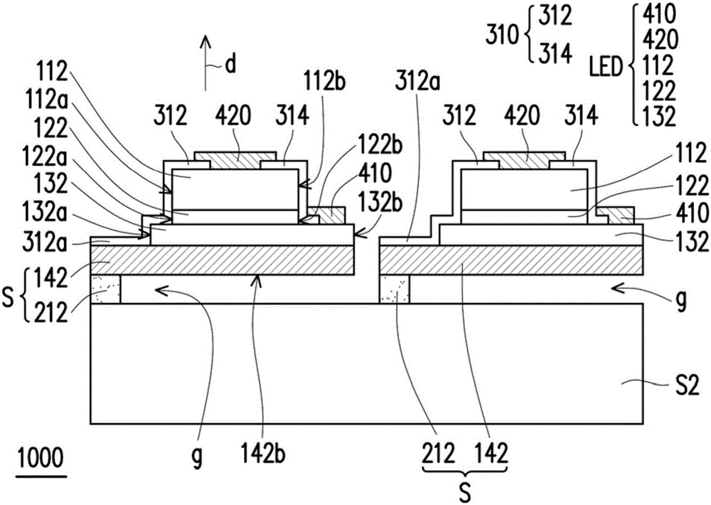
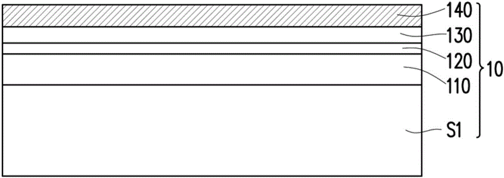
[0095] Figure 1A to Figure 1J It is a schematic cross-sectional view of a manufacturing method of a micro LED device according to an embodiment of the present invention. Figure 1A to Figure 1H It is a schematic cross-sectional view of the manufacturing method of the micro-LED intermediary structure. Please refer to Figure 1A , firstly, a semiconductor structure 10 is provided. The semiconductor structure 10 includes multiple semiconductor layers (not labeled) and a first sacrificial layer 140 stacked on the inner surface of the growth substrate S1 in sequence. The first sacrificial layer 140 is disposed on the multi-layer semiconductor. The multilayer semiconductor includes a first-type semiconductor layer 130 and a second-type semiconductor layer 110 opposite in polarity to the first-ty...


PUM


Abstract

The invention provides a manufacturing method of an intermediate structure of a micro-LED unit. A micro-LED is formed on a growing substrate. A transfer substrate is provided and a sacrificial layer is formed on the transfer substrate. Then, the micro-LED is transferred to the substrate. At least a portion of the sacrificial layer on the transfer substrate is removed so that there is a gap between the micro-LED and the transfer substrate. The untreated sacrificial layer temporarily holds the micro-LED on the transfer substrate.

Description

technical field [0001] The present invention relates to a photoelectric element and its manufacturing method, and in particular to a micro-LED unit intermediary structure and its manufacturing method, a micro-LED unit, its manufacturing method, and a micro-LED device. Background technique [0002] In the manufacturing process of the existing micro light-emitting diode intermediary structure, it is often necessary to use extremely high-precision and expensive transposition tips, which makes mass production difficult and the production cost is too high. Moreover, the general manufacturing method of the micro-LED intermediary structure requires multiple transposition actions. The multiple transposition actions are time-consuming and labor-intensive, and are detrimental to the manufacturing yield of the micro-LED units. Contents of the invention [0003] The invention provides a micro light emitting diode device, a micro light emitting diode unit and a manufacturing method th...

Claims


Application Information

Patent Timeline
IPC IPC(8): H01L21/77H01L27/15
CPCH01L21/77H01L27/15
Inventor 吴宗典张正杰罗国隆林炳昌
Owner AU OPTRONICS CORP
Why Eureka
Try Eureka