
FPGA (Field Programmable Gate Array) circuit and window signal adjustment method

A circuit and signal technology, applied in the field of FPGA circuit and window signal adjustment, can solve the problems of large adjustment range, low accuracy and efficiency, and achieve the effect of good matching and improving adjustment efficiency.

Active Publication Date: 2017-06-13
SHENZHEN PANGO MICROSYST CO LTD
View PDF10 Cites 3 Cited by
  • Summary
  • Abstract
  • Description
  • Claims
  • Application Information

AI Technical Summary

Problems solved by technology

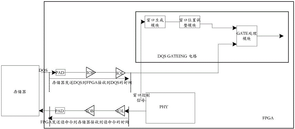
[0004] The technical problem mainly solved by the present invention is to provide an FPGA circuit and a window signal adjustment method to solve the problems in the prior art that when adjusting the window signal, the adjustment range is relatively large, and the adjustment accuracy and efficiency are relatively low.

Method used


Image

  • FPGA (Field Programmable Gate Array) circuit and window signal adjustment method
  • FPGA (Field Programmable Gate Array) circuit and window signal adjustment method
  • FPGA (Field Programmable Gate Array) circuit and window signal adjustment method

Examples


Embodiment 1

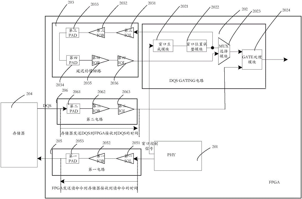
[0047] This embodiment provides a kind of FPGA circuit, see figure 2 , figure 2 The schematic diagram that a kind of FPGA circuit that this embodiment provides is connected with external memory; figure 2 Among them, the external memory 204 is connected with the FPGA circuit; the FPGA circuit includes:

[0048] PHY201, DQS GATING circuit 202 connected to PHY 201, delay compensation loop 203 connected to DQS GATING circuit 202, first circuit 205 connected between PHY201 and external memory 204, connected between external memory 204 and DQS GATING circuit 202 Between the second circuit 206; where,

[0049] Both ends of the delay compensation loop 203 are respectively connected to both ends of the DQS GATING circuit 202;

[0050] PHY201, used to send a read command to the external memory 204 through the first circuit 205, and at the same time send a window control signal to the DQS GATING circuit 202;

[0051] Optionally, the first circuit 205 includes a first IOL2051, a fi...

Embodiment 2

[0084] This embodiment provides a window signal adjustment method, which is applied to the FPGA circuit in Embodiment 1, PHY201, DQS GATING circuit 202 connected to PHY 201, delay compensation circuit 203 connected to DQS GATING circuit 202, connected between PHY201 and external The first circuit 205 between the memory 204, the second circuit 206 connected between the external memory 204 and the DQS GATING circuit 202; the two ends of the delay compensation loop 203 are respectively connected with the two ends of the DQS GATING circuit 202; see Figure 7 , Figure 7 It is a flowchart of a window signal adjustment method provided in this embodiment, and the window signal adjustment method includes the following steps:

[0085] S701: The PHY 201 sends a read command to the external memory 204 through the first circuit 205, and simultaneously sends a window control signal to the DQS GATING circuit 202;

[0086] Optionally, the first circuit 205 includes a first IOL2051, a first IO...


PUM


Abstract

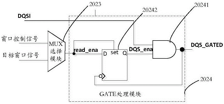
The invention provides an FPGA (Field Programmable Gate Array) circuit and a window signal adjustment method. The FPGA circuit comprises a physical layer, a DQS (Data Strobe Signal) GATING circuit, a delay compensation loop, a first circuit and a second circuit, wherein the DQS GATING circuit is connected with the physical layer; the delay compensation loop is connected with the DQS GATING circuit; the first circuit is connected between the physical layer and an external storage; the second circuit is connected between the external storage and the DQS GATING circuit; a window control signal emitted by the physical layer can sequentially pass through the DQS GATING circuit and the delay compensation loop; the DQS GATING circuit is used for adjusting the position of a target window signal relative to a DQS according to the target window signal and the DQS. By adopting the scheme, the window control signal passes through the delay compensation loop, so that the time from emitting a read command by the physical layer to receiving the read command by the external storage and the time from sending the DQS by the external storage to receiving the DQS by the DQS GATING circuit are compensated; through the compensation, when the position of an initial window signal is near the DQS, the window signal can be rapidly adjusted to a reasonable position, and the adjusting efficiency of the window signal is increased.

Description

technical field [0001] The invention relates to the field of integrated circuit design, in particular to an FPGA (Field-Programmable Gate Array, Field Programmable Gate Array) circuit and a window signal adjustment method. Background technique [0002] In DDR (Double Data Rate, double rate synchronous dynamic random access memory) memory, its input and output data are synchronized with the rising and falling edges of the clock, so a bidirectional DQS (Data Strobe) with the same frequency as the clock is required in the read and write operations. Signal, data strobe signal) signal to grab data. This DQS signal is a three-state signal, which is in a high-impedance state when not in use. When the memory receives a read command, the DQS signal will switch to logic low in the previous cycle of data output. When the read command is completed, it will be at the end of the DQS signal. The DQS signal returns to the high-impedance state after half a clock period after a falling edge ...

Claims


Application Information

Patent Timeline
IPC IPC(8): G11C7/10
CPCG11C7/1066G11C7/1093
Inventor 马硝霞
Owner SHENZHEN PANGO MICROSYST CO LTD
Learn More