
Multispectral chip based on meta-surface narrow-band filtering and preparation method thereof

A narrow-band filter and metasurface technology, applied in the field of spectrum chips, can solve problems such as the difficulty of process realization, and achieve the effect of wide applicability and easy realization

Active Publication Date: 2017-06-13
XI'AN INST OF OPTICS & FINE MECHANICS - CHINESE ACAD OF SCI
View PDF6 Cites 44 Cited by
  • Summary
  • Abstract
  • Description
  • Claims
  • Application Information

AI Technical Summary

Problems solved by technology

Both filter designs use the principle of multi-beam interference filtering. When multi-spectral filtering is to be achieved, a specific film thickness or film number needs to be selected for a specific wavelength, so it needs to be on the same chip. It is very difficult to realize the preparation of filter unit arrays with different film thicknesses

Method used


Image

  • Multispectral chip based on meta-surface narrow-band filtering and preparation method thereof
  • Multispectral chip based on meta-surface narrow-band filtering and preparation method thereof
  • Multispectral chip based on meta-surface narrow-band filtering and preparation method thereof

Examples


Embodiment Construction

[0026] The present invention will be further described below in conjunction with the accompanying drawings.

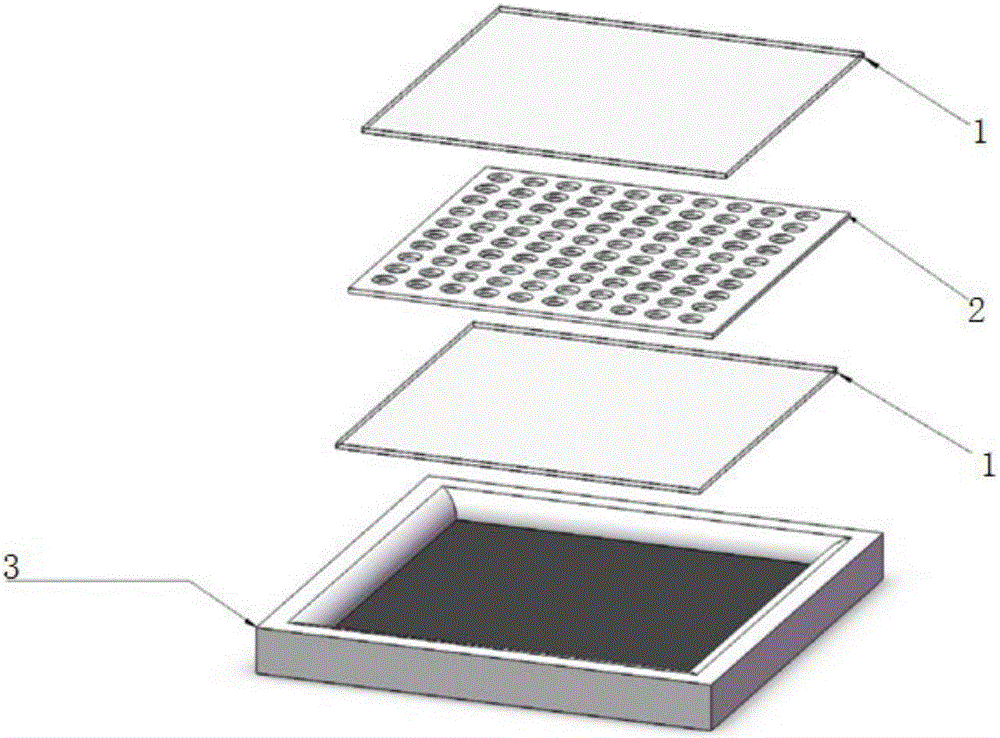
[0027] The present invention proposes an area array multispectral chip based on metasurface narrow-band filtering, by preparing a metasurface structure on the surface of an area array COMS image sensor, that is, a metal nanostructure, and utilizing the surface plasmon effect of the metal nanostructure to realize narrow-band filtering Light, and then capture more accurate and detailed map texture information of the target object.

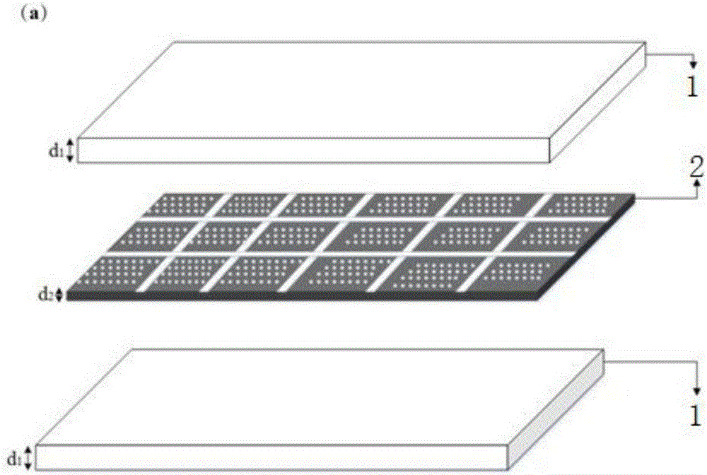
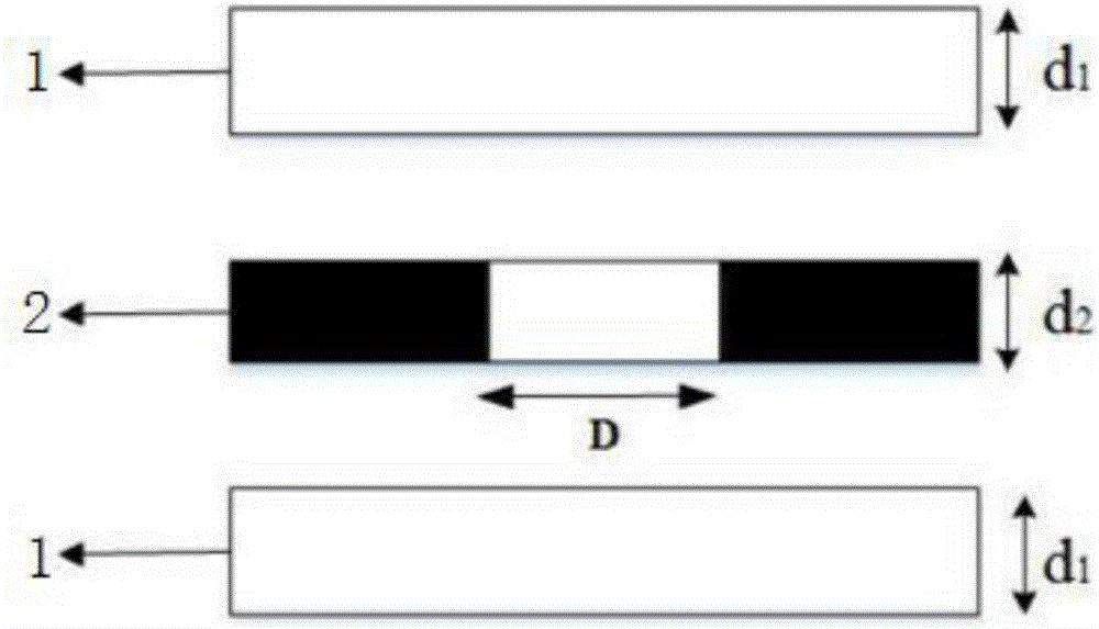
[0028] like figure 1 As shown, the spectrum chip of the present invention is mainly composed of an area array image sensor and a metasurface structure filter array. The metasurface structure filter is mainly composed of three parts: the passivation layer of nano-membrane, the periodic array structure of metal nanoholes, and the passivation layer of nano-membrane. The optical signal of the target object presents image information on the surf...


PUM


Abstract

The invention provides a multispectral chip based on meta-surface narrow-band filtering. The chip comprises an area array image sensor and a meta-surface structure light filter array. The meta-surface structure light filter array comprises two nanometer film passivation layers and a metal nanopore periodic array structure located between the two nanometer film passivation layers. The meta-surface structure light filter array is located on the area array image sensor. The metal nanopore periodic array structure comprises a metal dielectric film layer. The metal dielectric film layer is provided with periodic nanopore arrays of different sizes. The periodic nanopore nanometer structure arrays of different sizes are prepared on the metal dielectric film layer of the same thickness, and narrow-band filtering of the target image on the multispectral coverage is achieved. The multispectral chip is applicable to finer atlas information collection, the metal nanometer periodic structure is prepared on the surface of the image sensor, the area array multispectral chip is achieved, the chip is easy to obtain technologically, and the wide application range is achieved.

Description

technical field [0001] The present invention relates to a multi-spectral chip based on metasurface narrow-band filtering, in particular to a spectral chip based on metal nanostructure surface plasmon resonance and surface plasmon localized enhanced transmission effect narrow-band filtering and its realization technology . Background technique [0002] The metasurface narrowband filter is an interference filter based on the metal nanostructure surface plasmon resonance and the surface plasmon localization enhanced transmission effect, that is, changing the size and period of the metal nanostructure array on a single plane to adjust Its filtering properties, and then realize the fine wavelength selection of the spectrum of the target image, and accurately capture the spectral curve of the target spectral texture, so as to obtain valuable object attribute information. As a commonly used image sensor, the spectral chip is widely used in scientific research fields such as materi...

Claims


Application Information

Patent Timeline
IPC IPC(8): H01L27/146H01L27/148B82Y40/00
CPCB82Y40/00H01L27/14625H01L27/14685H01L27/14806
Inventor 鱼卫星杨靖忠仝晓刚胡炳樑
Owner XI'AN INST OF OPTICS & FINE MECHANICS - CHINESE ACAD OF SCI
Learn More