Thin film transistor, preparation method of thin film transistor and liquid crystal display panel

A technology for thin film transistors and manufacturing methods, which is applied in the fields of transistors, semiconductor/solid-state device manufacturing, semiconductor devices, etc., can solve the problems of cumbersome manufacturing process, reducing aperture ratio, limiting the switching ratio of TFT devices, etc., so as to reduce the process flow and improve the switching ratio. , the effect of improving the opening rate

Inactive Publication Date: 2017-06-13
TCL CHINA STAR OPTOELECTRONICS TECH CO LTD
View PDF3 Cites 11 Cited by
  • Summary
  • Abstract
  • Description
  • Claims
  • Application Information

AI Technical Summary

Problems solved by technology

[0002] At present, most semiconductor channels of TFT devices in TFT (thin film transistor) array substrates adopt two-dimensional planar structures, and the length of the channels will be relatively long, thereby limiting the switching ratio of TFT devices; the size of TFT devices in TFT array substrates It will be made relatively large, resulting in a reduction in the aperture ratio; in the TFT manufacturing process, multiple masks (generally at least 5 masks) are required, the process is cumbersome and the cost is high
These all restrict the development of TFT array substrates

Method used


Image

  • Thin film transistor, preparation method of thin film transistor and liquid crystal display panel
  • Thin film transistor, preparation method of thin film transistor and liquid crystal display panel
  • Thin film transistor, preparation method of thin film transistor and liquid crystal display panel

Examples


Embodiment Construction

[0022] The present invention will be described in further detail below in conjunction with the accompanying drawings and embodiments.

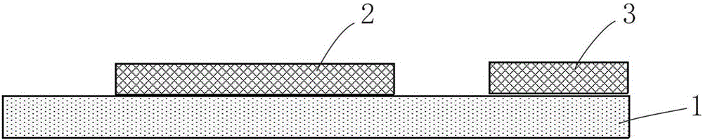
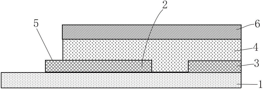
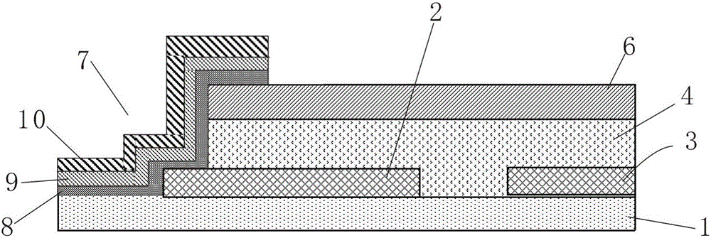
[0023] like image 3 and Figure 4 As shown, a thin film transistor of the present invention includes a substrate 1 on which a patterned source (Source) 2 and a patterned common electrode (COM) 3 are deposited, and the source 2 and the common electrode 3 are arranged on the same layer, and the source electrode 2 and the common electrode 3 are covered with a spacer layer (Spacer) 4, and the side of the source electrode 2 away from the common electrode 3 ( image 3 The left side of the liner layer 4 is exposed to form an exposed part 5, and a drain electrode (Drain) is deposited on the liner layer 4 and patterned to form a pixel electrode 6, which is located on one side of the source electrode 2 ( image 3 On the left side of ), the exposed part 5 and the substrate 1 are located on the side of the source 2, and a patterned semiconductor layer ...


PUM


Abstract

The invention provides a thin film transistor. The thin film transistor comprises a substrate, a patterned source electrode and a patterned common electrode are deposited on the substrate, and a liner layer covers the source electrode and the common electrode. The side, away from the common electrode, of the source electrode is exposed outside the liner layer to form an exposed part, a drain electrode is deposited on the liner layer and patterned to form a pixel electrode, and the pixel electrode is located on the side of the source electrode. A patterned semiconductor layer, a grid electrode insulation layer and a patterned grid electrode are sequentially deposited on the exposed part and on the side, located on the source electrode, of the substrate respectively so as to form a semiconductor channel with a section of a stepped structure, and the pixel electrode is connected with the source electrode through the semiconductor layer. The invention further provides a preparation method of the thin film transistor and a liquid crystal display panel. Compared with the prior art, the on-off ratio of the thin film transistor is improved, and the aperture opening ratio is also improved. The thin film transistor can be used on a high-resolution panel; the technology process is shortened, and the cost is saved.

Description

technical field [0001] The invention relates to the field of display technology, in particular to a thin film transistor based on an IPS structure, a manufacturing method thereof, and a liquid crystal panel. Background technique [0002] At present, most semiconductor channels of TFT devices in TFT (thin film transistor) array substrates adopt two-dimensional planar structures, and the length of the channels will be relatively long, thereby limiting the switching ratio of TFT devices; the size of TFT devices in TFT array substrates It will be made relatively large, resulting in a reduction in the aperture ratio; in the TFT manufacturing process, it is necessary to use multiple masks (generally at least 5 masks), the process is cumbersome and the cost is high. All of these restrict the development of TFT array substrates. Contents of the invention [0003] In order to overcome the deficiencies of the prior art, the invention provides a thin film transistor and its manufact...

Claims


Application Information

Patent Timeline
Patent Type & Authority Applications(China)
IPC IPC(8): H01L29/786H01L29/417H01L21/336H01L21/34H01L27/12
CPCH01L27/1222H01L27/1225H01L29/41733H01L29/6675H01L29/66969H01L29/78663H01L29/7869H01L29/78696G02F1/134363G02F1/136286G02F1/1368H01L29/78642H01L27/124G02F1/134318G02F1/1343H01L27/1214G02F2201/123G02F2201/121G02F1/1339
Inventor 黄贵华
Owner TCL CHINA STAR OPTOELECTRONICS TECH CO LTD
Why Eureka
Try Eureka