Display device and electronic device

a display device and electronic device technology, applied in semiconductor devices, electrical devices, instruments, etc., can solve the problems of adverse effects of semiconductor film on transistor characteristics, transistor characteristics are affected, etc., and achieve excellent switching characteristics, high on/off ratio, and high operation speed

Active Publication Date: 2018-03-15
SEMICON ENERGY LAB CO LTD
View PDF2 Cites 12 Cited by
  • Summary
  • Abstract
  • Description
  • Claims
  • Application Information

AI Technical Summary

Benefits of technology

[0009]In the case where a plurality of different circuits are formed on an insulating surface (e.g., in the case where a pixel portion and a driver circuit are formed over the same substrate) to manufacture a display device, excellent switching characteristics such as a high on / off ratio are needed for a transistor used for the pixel portion, and high operation speed is needed for a transistor used for the driver circuit. In particular, the higher the resolution of a display device is, as in an ultra-high-definition (also referred to as 4K resolution, 4K2K, or 4K) display device or a super-high-definition (also referred to as 8K resolution, 8K4K, or 8K) display device, the shorter the writing time of a display image is; thus, it is preferable that the transistor used for the driver circuit operate at high speed.
[0010]In view of the foregoing problems, an object of one embodiment of the present invention is to improve the field-effect mobility and reliability of a transistor including a metal oxide film. Another object of one embodiment of the present invention is to inhibit a change in the electrical characteristics of a transistor including a metal oxide film and to improve the reliability of the transistor. Another object of one embodiment of the present invention is to provide a display device with high display quality and high resolution. Another object of one embodiment of the present invention is to provide a display device with reduced power consumption. Another object of one embodiment of the present invention is to provide a novel display device. Another object of one embodiment of the present invention is to provide a novel electronic device.

Problems solved by technology

However, when the field-effect mobility is increased, the transistor has a problem with its characteristics, that is, the transistor tends to be normally on.
Furthermore, in a transistor that uses an oxide semiconductor film in a channel region, oxygen vacancies which are formed in the oxide semiconductor film adversely affect the transistor characteristics.

Method used


Image

  • Display device and electronic device
  • Display device and electronic device
  • Display device and electronic device

Examples


embodiment 1

[0109]In this embodiment, a display device of one embodiment of the present invention and a method for manufacturing the display device will be described with reference to FIGS. 1A-1, 1A-2, 1B-1, and 1B-2, FIGS. 2A and 2B, FIG. 3, FIGS. 4A-1, 4A-2, 4B-1, and 4B-2, FIGS. 5A-1 to 5A-3 and 5B-1 to 5B-3, FIGS. 6A-1, 6A-2, 6B-1, and 6B-2, FIGS. 7A-1, 7A-2, 7B-1, and 7B-2, FIGS. 8A-1, 8A-2, 8B-1, and 8B-2, FIGS. 9A and 9B, FIGS. 10A-1, 10A-2, 10B-1, and 10B-2, FIGS. 11A-1, 11A-2, 11B-1, and 11B-2, FIGS. 12A-1, 12A-2, 12B-1, and 12B-2, FIGS. 13A-1 and 13B-1, FIGS. 14A to 14C, FIGS. 15A to 15C, and FIGS. 16A and 16B.

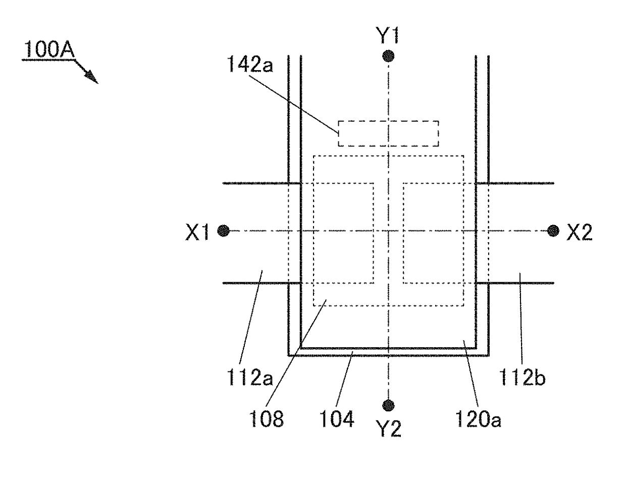
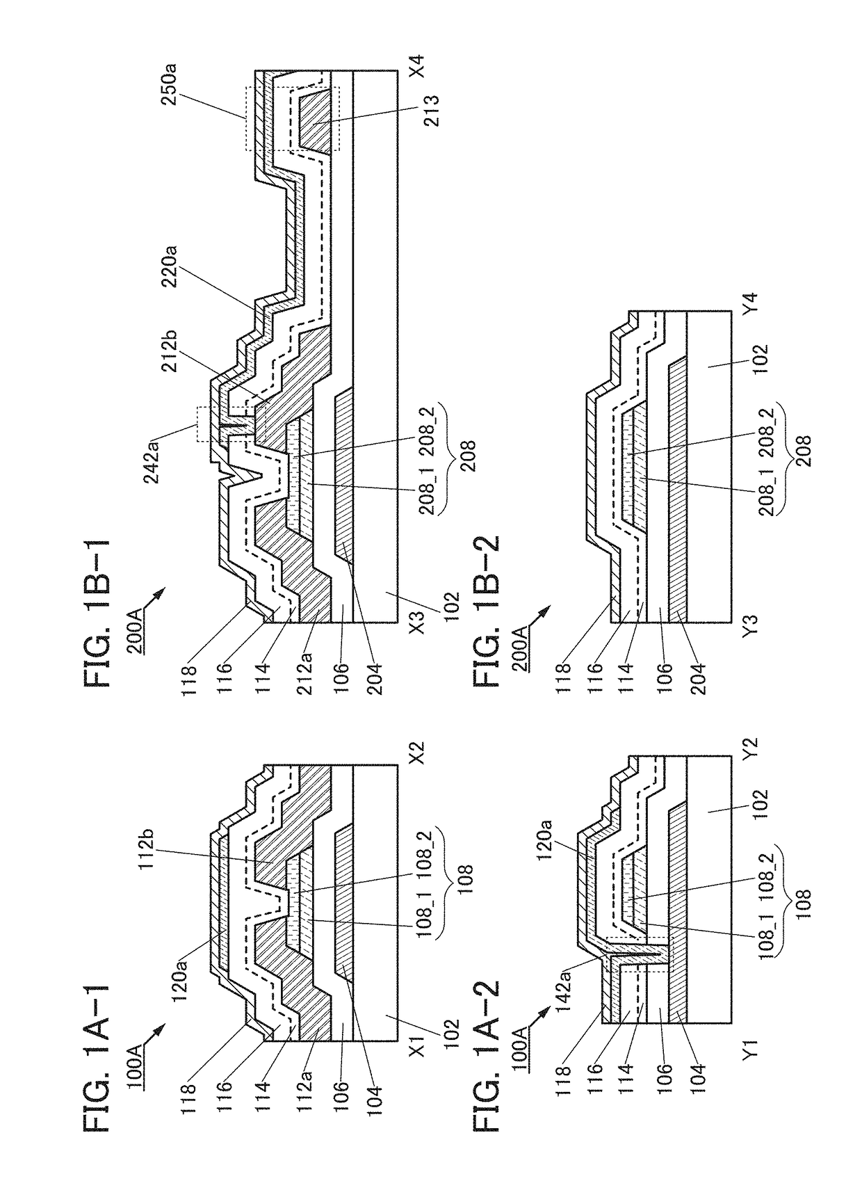
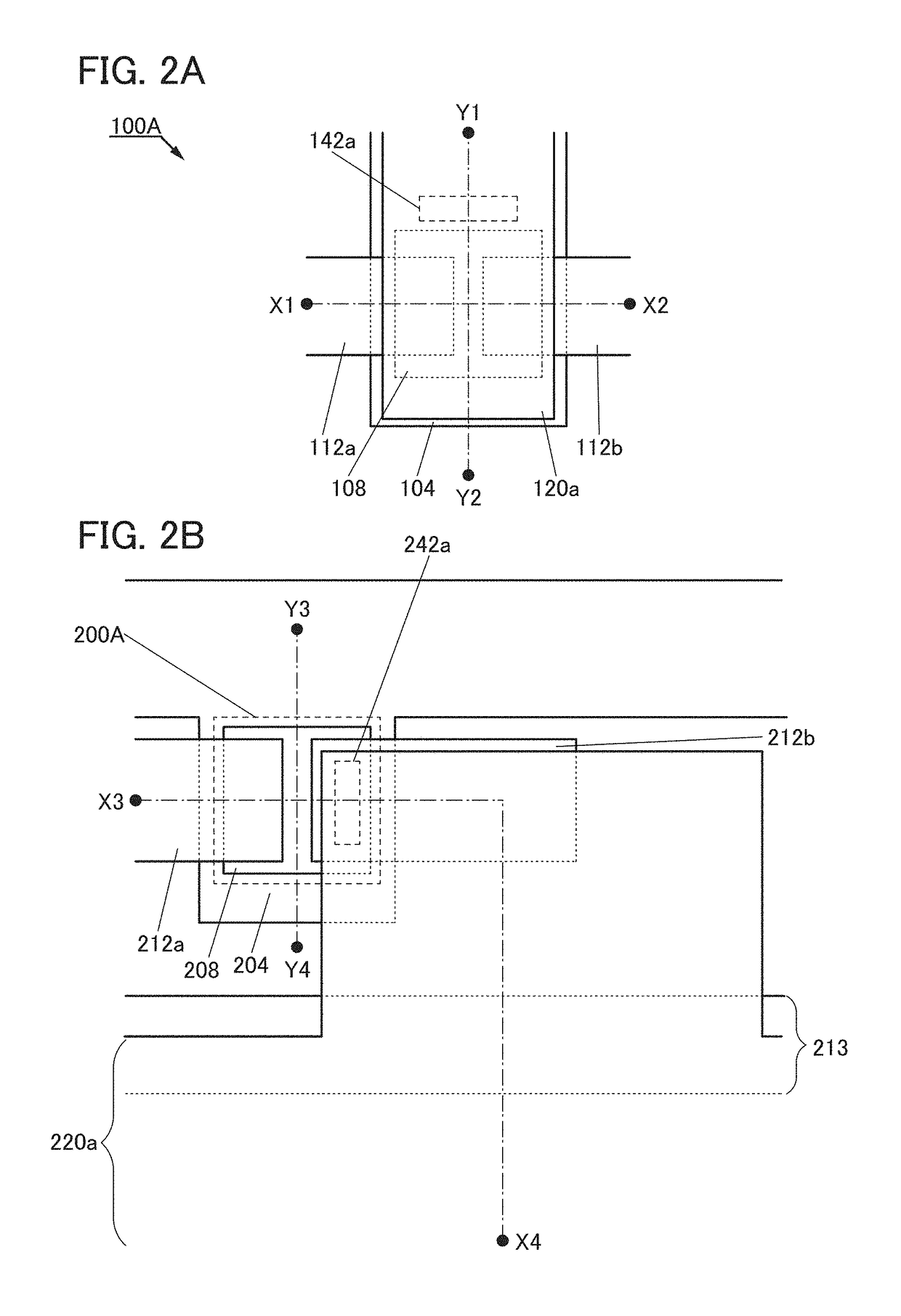
[0110]FIGS. 2A and 2B are top views of transistors included in a driver circuit and a display portion of a display device of one embodiment of the present invention. FIG. 2A is a top view of a transistor 100A included in the driver circuit, and FIG. 2B is a top view of a transistor 200A included in a pixel portion. FIG. 1A-1 corresponds to a cross-sectional view taken along dash...

embodiment 2

[0315]In this embodiment, the metal oxide film of one embodiment of the present invention will be described with reference to FIG. 18, FIGS. 19A to 19L, and FIGS. 20A to 20C.

[0316]Described below is the detail of a metal oxide having a CAC composition that can be used in the transistor disclosed in one embodiment of the present invention. As a typical example of the metal oxide having a CAC composition, a CAC-OS will be described here.

[0317]In the CAC-OS, as illustrated in FIG. 3 for example, elements contained in the metal oxide are unevenly distributed to form the regions 001 and 002 each containing any of the elements as a main component. The regions are mixed to form or to be distributed in a mosaic pattern. In other words, the CAC-OS has a composition in which elements included in a metal oxide are unevenly distributed. Materials including unevenly distributed elements each have a size of greater than or equal to 0.5 nm and less than or equal to 10 nm, preferably greater than o...

embodiment 3

[0381]In this embodiment, a display device using a horizontal electric field mode liquid crystal element as a display element is described with reference to FIG. 21.

[0382]FIG. 21 shows flow charts showing manufacturing processes of display devices using horizontal electric field mode liquid crystal elements. FIG. 21 shows examples of manufacturing processes in the case of using an oxide semiconductor (in particular, CAC-OS), in the case of using low-temperature poly-silicon (LTPS), and in the case of using hydrogenated amorphous silicon (a-Si:H) as a channel of a transistor.

[0383]The case of using a CAC-OS in the transistor is described. First, a gate electrode (GE) is formed with a sputtering apparatus (SP). Note that one mask is used when the gate electrode is processed.

[0384]Then, a gate insulating film (GI: gate insulator) is formed over the gate electrode with a PECVD apparatus. After that, an oxide semiconductor (OS) film to be an active layer is formed over the gate insulatin...


PUM


Abstract

A novel display device is provided. The display device includes a pixel portion and a driver circuit for driving the pixel portion. The driver circuit includes a first transistor having a dual-gate structure. The pixel portion includes a second transistor having a single-gate structure and a pixel electrode electrically connected to the second transistor. The first transistor and the second transistor each include a first metal oxide film functioning as a channel. The metal oxide films each include a first region and a second region. The first region contains In or Zn, and oxygen. The second region contains In or an element M, and oxygen. The first region and the second region are dispersed or distributed in a mosaic pattern.

Description

TECHNICAL FIELD[0001]One embodiment of the present invention relates to a display device and an electronic device.[0002]Note that one embodiment of the present invention is not limited to the above technical field. The technical field of one embodiment of the invention disclosed in this specification and the like relates to an object, a method, or a manufacturing method. In addition, one embodiment of the present invention relates to a process, a machine, manufacture, or a composition of matter. In particular, one embodiment of the present invention relates to a semiconductor device, a display device, a light-emitting device, a power storage device, a storage device, a driving method thereof, or a manufacturing method thereof.[0003]In this specification and the like, a semiconductor device generally means a device that can function by utilizing semiconductor characteristics. A semiconductor element such as a transistor, a semiconductor circuit, an arithmetic device, and a memory dev...

Claims


Application Information

Patent Timeline
Patent Type & Authority Applications(United States)
IPC IPC(8): H01L27/12
CPCH01L27/1225H01L27/1255H01L27/1248H01L27/124H01L27/0251G09G2340/0407G09G3/3677G09G3/3688G09G2330/021G09G3/3233G09G3/3648G09G5/39G09G2320/103G09G2330/04G09G2360/144G09G2360/18H01L29/78648H01L29/7869H01L29/78696
Inventor YAMAZAKI, SHUNPEIKOEZUKA, JUNICHIOKAZAKI, KENICHI
Owner SEMICON ENERGY LAB CO LTD
Why Eureka
Try Eureka