Gate tube material, gate tube device and preparation method thereof

A technology of gating tubes and devices, which is applied in the field of Wiener Electronics, can solve the problems of insufficient on-state loadable current, high threshold voltage of gating tubes, high off-state leakage current, etc., to reduce power consumption, reduce on-voltage, The effect of increasing the switching ratio

Inactive Publication Date: 2019-04-16
HUAZHONG UNIV OF SCI & TECH
View PDF8 Cites 13 Cited by
  • Summary
  • Abstract
  • Description
  • Claims
  • Application Information

AI Technical Summary

Problems solved by technology

This solves the technical problems of the existing gating tube with too high threshold voltage, low on-off ratio, insufficient on-state loadable current and high off-state leakage current

Method used


Image

  • Gate tube material, gate tube device and preparation method thereof
  • Gate tube material, gate tube device and preparation method thereof
  • Gate tube material, gate tube device and preparation method thereof

Examples


preparation example Construction

[0044] The present invention provides a method for preparing the above gating tube device unit, comprising the following steps:

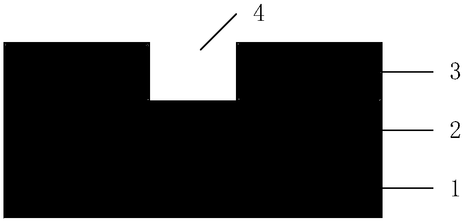
[0045] (1) preparing the first metal electrode layer on the substrate;

[0046] (2) An insulating layer is prepared on the first metal electrode layer, and the insulating layer is patterned to obtain a hole structure, and part of the first metal electrode layer at the bottom is exposed through the hole structure; Photolithography or electron beam lithography (EBL) is used to form patterns, and then conductance coupled plasma etching (ICP) is used to obtain patterns of different shapes.

[0047] (3) preparing a gating layer on the exposed first metal electrode layer, filling the hole structure, and the material used in the gating layer is the gating tube material as described above;

[0048] (4) A second metal electrode layer is prepared on the insulating layer filled with the hole structure, and the first metal electrode layer and the second metal ...

Embodiment 1

[0052] This implementation example provides a gating tube material, which is characterized in that: the general chemical formula of the gating tube material can be expressed as Ge x Te y A 100-x-y (where A refers to one of the elements C, B, Si, Al, Sb, Bi), x, y are the atomic percentage of the element and 10≤x<60, 40

[0053] Preferably, in the Ge x Te y A 100-x-y (where A refers to one of the elements C, B, Si, Al, Sb, Bi), the element C is selected to form Ge x Te y C 100-x-y , and 10≤x<60, 40

[0054] More preferably, in the Ge x Te y A 100-x-y (where A refers to one of the elements C, B, Si, Al, Sb, Bi), the element C is selected to form Ge x Te y C 100-x-y , and 20≤x≤45, 55

[0055] More specifically, the material thickness of the gate tube is 1-200 nm. Preferably, in this implementation case, the material thickness of the gate tube is 120nm; of course, in other implementation cases, the materi...

Embodiment 2

[0060] This embodiment also provides a method for manufacturing the gating tube material as described in Embodiment 1, according to the schematic formula Ge of the general chemical formula x Te y A 100-x-y (Among them, A refers to one of the elements C, B, Si, Al, Sb, Bi). The gate tube material is prepared by enhanced chemical vapor deposition, low pressure chemical vapor deposition, metal compound vapor deposition, molecular beam epitaxy, atomic vapor deposition, and atomic layer deposition.

[0061] Preferably, in this embodiment, the selected element C constitutes Ge x Te y C 100-x-y thin films, and prepared Ge by magnetron co-sputtering x Te y C 100-x-y thin film; more preferably, the Ge x Te y C 100-x-y Thin film is Ge 20 Te 65 C 15 film.

[0062] Specifically: use Ge 25 Te 75 Alloy target, Ge 50 Te 50 Co-sputtering of alloy target and C target to deposit a certain thickness of Ge 20 Te 65 C 15 Thin film, the process parameters are: pumping to the ba...


PUM


Abstract

The invention belongs to the technical field of Wiener electronics, and particularly relates to a gate tube material, a gate tube device and a preparation method of the gate tube device. The gate tubedevice comprises a first metal electrode layer, a second metal electrode layer and a gate layer between the two electrode layers. The chemical general formula of the gate layer material can be shownas GexTeyA100-x-y, where A in the formula is one of the elements C, B, Si, Al, Sb and Bi, x and y are atomic percentages of elements, x is greater than or equal to 10 and less than 60, y is greater than 40 and less than 90, and 100-x-y is greater than 0 and less than or equal to 25. The gate tube provided by the invention has the advantages of simplicity in preparation, capability of driving ultra-high on-state current (more than 11mA), low off-state current, high switching ratio, high switching speed and low on-voltage.

Description

technical field [0001] The invention belongs to the technical field of Wiener electronics, and in particular relates to a gating material, a gating tube device and a preparation method thereof. Background technique [0002] Semiconductor memory devices are one of the pillars of the information age. The next-generation new non-volatile memory such as phase-change memory, resistive change memory and other devices have become the most popular next-generation memory due to their extremely fast erasing and writing speed, excellent miniaturization performance, and three-dimensional stacking. Today, when Moore's Law is becoming invalid, in order to further increase the storage density, three-dimensional stacking of memory cells has become a very effective solution. The gating tube is the core device to achieve high-density large-scale array integration, reduce operating power consumption, and reduce the effective cell area; among them, the two-terminal gating tube device can be ve...

Claims


Application Information

Patent Timeline
Patent Type & Authority Applications(China)
IPC IPC(8): H01L45/00
CPCH10N70/8828H10N70/011
Inventor 童浩何达缪向水林琪
Owner HUAZHONG UNIV OF SCI & TECH
Why Eureka
Try Eureka