High-mobility transistor based on PMMA doped micro-molecule and preparation method thereof

A high-mobility, transistor-based technology, applied in the field of organic electronics, can solve problems such as hindering the further use of devices, large surface roughness, and reduced mobility, and achieve the effects of easy industrialization, simple preparation methods, and improved device performance

Active Publication Date: 2017-09-22
SOUTH CHINA NORMAL UNIVERSITY
View PDF8 Cites 12 Cited by
  • Summary
  • Abstract
  • Description
  • Claims
  • Application Information

AI Technical Summary

Problems solved by technology

But for now, there are still some problems to be solved: (1) The solubility of small organic molecules is poor, and the solution method is difficult to prepare; (2) The mobility of the prepared devices is low, generally within 1cm 2 Below / (V S), the switching ratio is low, which hinders the further use of the device; (3) the active layer prepared by the solution method has many defects on the surface, the film continuity is not good, and the surface roughness is large, which seriously affects the current carrying (4) The combination of the active layer and the insulating layer is not good, resulting in poor electrical stability of the device

Method used


Image

  • High-mobility transistor based on PMMA doped micro-molecule and preparation method thereof
  • High-mobility transistor based on PMMA doped micro-molecule and preparation method thereof
  • High-mobility transistor based on PMMA doped micro-molecule and preparation method thereof

Examples


Embodiment 1

[0036] A method for preparing a high-mobility transistor based on PMMA-doped small molecules described in this embodiment comprises the following steps:

[0037] S1: Preparation of C8-BTBT and PMMA mixed solution: use C8-BTBT and PMMA as solute and chlorobenzene as solvent to prepare a mixed solution of 0.5% mass ratio of C8-BTBT and 0.5% mass ratio of PMMA, and the prepared solution is sonicated for 10 minutes use, ready-to-use;

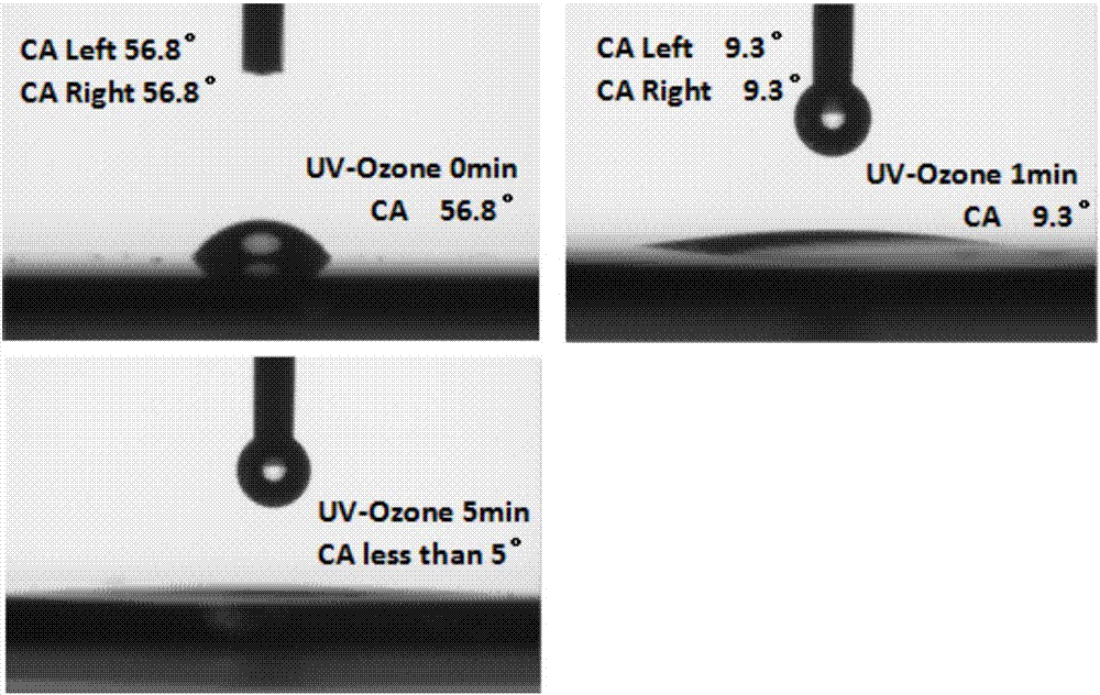
[0038] S2: Substrate cleaning: Select a P-type heavily doped silicon wafer containing silicon dioxide, cut it into a square with a side length of 1.5 cm with a silicon wafer knife, and clean it by ultrasonic: put acetone, isopropanol, and Deionized water, acetone, isopropanol, deionized water, and then rinse it with deionized water for two minutes to remove impurities such as organic matter on the surface, spray nitrogen with a nitrogen gun to dry the surface of the silicon wafer with deionized water, and then It is dried in an oven;

[0039] S3: ...

Embodiment 2

[0046] A method for preparing a high-mobility transistor based on PMMA-doped small molecules described in this embodiment comprises the following steps:

[0047] S1: Preparation of C8-BTBT and PMMA mixed solution: use C8-BTBT and PMMA as solute and chlorobenzene as solvent to prepare a mixed solution of 0.5% mass ratio of C8-BTBT and 0.5% mass ratio of PMMA, and the prepared solution is sonicated for 10 minutes use, ready-to-use;

[0048] S2: Substrate cleaning: Select a P-type heavily doped silicon wafer containing silicon dioxide, cut it into a square with a side length of 1.5 cm with a silicon wafer knife, and clean it by ultrasonic: put acetone, isopropanol, and Deionized water, acetone, isopropanol, deionized water, and then rinse it with deionized water for two minutes to remove impurities such as organic matter on the surface, spray nitrogen with a nitrogen gun to dry the surface of the silicon wafer with deionized water, and then It is dried in an oven;

[0049] S3: ...

Embodiment 3

[0055] A method for preparing a high-mobility transistor based on PMMA-doped small molecules described in this embodiment comprises the following steps:

[0056] S1: Preparation of C8-BTBT and PMMA mixed solution: use C8-BTBT and PMMA as solute and chlorobenzene as solvent to prepare a mixed solution of 0.5% mass ratio of C8-BTBT and 0.5% mass ratio of PMMA, and the prepared solution is sonicated for 10 minutes use, ready-to-use;

[0057] S2: Substrate cleaning: Select a P-type heavily doped silicon wafer containing silicon dioxide, cut it into a square with a side length of 1.5 cm with a silicon wafer knife, and clean it by ultrasonic: put acetone, isopropanol, and Deionized water, acetone, isopropanol, deionized water, and then rinse it with deionized water for two minutes to remove impurities such as organic matter on the surface, spray nitrogen with a nitrogen gun to dry the surface of the silicon wafer with deionized water, and then It is dried in an oven;

[0058] S3: ...


PUM


Abstract

The invention relates to a preparation method of a high-mobility transistor based on PMMA doped micro-molecule. The preparation method comprises the following steps: S1, preparing a C8-BTBT and PMMA mixed solution; S2, cleaning a substrate: selecting a P-type heavily-doped silicon slice containing silicon dioxide, cleaning the P-type heavily-doped silicon slice after tailoring the same; S3, preparing a C8-BTBT active layer and a PMMA modification layer: overspreading the C8-BTBT and PMMA mixed solution configured through the step S1 on the substrate by using a dropper, spin-coating for 40s under the rotation speed of 2000-3000rpm; S4, thermally treating the spin-coated film; S5, preparing a molybdenum oxide buffer layer; and S6, preparing the source electrode and the drain electrode. The preparation method disclosed by the invention is simple, the prepared active layer is less in surface defect, the performance of the manufactured transistor device is improved.

Description

technical field [0001] The invention relates to the technical field of organic electronics, in particular to a high-mobility transistor based on PMMA-doped small molecules and a preparation method thereof. Background technique [0002] Organic electronic flexible devices have received extensive attention from academia and social industry in the past 30 years, and they are an important development direction for future flexible electronic display devices. Great progress has been made, such as organic field effect transistors, organic solar cells, biosensors, TFT arrays, organic light-emitting diodes, etc. At present, organic materials and devices have gradually moved from basic research to industrialization. In application production, they have the characteristics of simple manufacturing process, flexibility, variety and low cost; The energy consumption of the OTFT is also reduced, which highlights the huge advantages in flexible display; in the future, the size of OTFT devic...

Claims


Application Information

Patent Timeline
Patent Type & Authority Applications(China)
IPC IPC(8): H01L51/05H01L51/40
CPCH10K71/12H10K10/46
Inventor 陆旭兵韦尉尧刘俊明
Owner SOUTH CHINA NORMAL UNIVERSITY
Why Eureka
Try Eureka