Method for forming multi-image sensor module

A sensor module and image sensor technology, which is applied in semiconductor devices, electric solid state devices, radiation control devices, etc., can solve the problems of focusing ability, dynamic balance difficult to adapt to demand, process difficulty and high process cost, positioning accuracy and assembly accuracy are difficult Control and other issues

Active Publication Date: 2021-04-13
GALAXYCORE SHANGHAI
View PDF7 Cites 0 Cited by
  • Summary
  • Abstract
  • Description
  • Claims
  • Application Information

AI Technical Summary

Problems solved by technology

[0002] With the rapid development of consumer electronic products, the single image sensor module suitable for portable electronic devices has no advantages in some market segments, and the focusing ability and dynamic balance are difficult to meet the needs under certain circumstances.
Multi-image sensor modules have appeared in portable electronic devices. Multi-image sensor modules are mainly used in the main camera of smartphones. And the problem of deviation angle, it is difficult to control the positioning accuracy and assembly accuracy, which will bring unsolvable problems in the subsequent imaging process
[0003] In addition, in the process of forming the image sensor chip, it is necessary to form a color filter film on most of the surface of the pixel array, and not to form a color filter film in some areas. The existing method is relatively high in terms of process difficulty and process cost.

Method used


Image

  • Method for forming multi-image sensor module
  • Method for forming multi-image sensor module
  • Method for forming multi-image sensor module

Examples


Embodiment Construction

[0026] In the following detailed description of the preferred embodiment, reference is made to the accompanying drawings which form a part hereof. The accompanying drawings show, by way of example, specific embodiments in which the invention can be practiced. The illustrated embodiments are not intended to be exhaustive of all embodiments in accordance with the invention. It is to be understood that other embodiments may be utilized and structural or logical changes may be made without departing from the scope of the present invention. Accordingly, the following detailed description is not limiting, and the scope of the invention is defined by the appended claims.

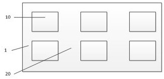
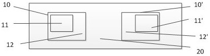
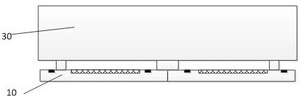
[0027] The present invention provides a method for forming a multi-image sensor module, comprising: S10 providing a wafer containing several image sensors; S20 cutting the wafer to form: an integrated multi-image sensor; respectively retaining dicing lane areas between the multi-image sensors ; S30 assembling the...


PUM


Abstract

The present invention provides a method for forming a multi-image sensor module, which is characterized in that the method includes: providing a wafer containing several image sensors; cutting the wafer to form: an integrated multi-image sensor; Reserving the dicing lane area respectively; assembling the integrated multi-image sensor to form a multi-image sensor module.

Description

technical field [0001] The invention relates to the field of semiconductor manufacturing, in particular to an assembly method of a multi-camera module. Background technique [0002] With the rapid development of consumer electronic products, the single image sensor module suitable for portable electronic devices has no advantage in some market segments, and the focusing ability and dynamic balance are difficult to meet the needs under certain circumstances. Multi-image sensor modules have appeared in portable electronic devices. Multi-image sensor modules are mainly used in the main camera of smartphones. And the problem of deviation angle, it is difficult to control the positioning accuracy and assembly accuracy, which will bring unsolvable problems in the subsequent imaging process. [0003] In addition, in the process of forming the image sensor chip, it is necessary to form a color filter film on most of the surface of the pixel array, and not to form a color filter fil...

Claims


Application Information

Patent Timeline
Patent Type & Authority Patents(China)
IPC IPC(8): H01L27/146
CPCH01L27/14685
Inventor 李杰
Owner GALAXYCORE SHANGHAI
Why Eureka
Try Eureka