Flip-chip LED device with wafer-level packaging, segmentation unit and manufacturing method thereof

A LED device, wafer-level technology, applied in electrical components, semiconductor devices, circuits, etc., can solve problems such as efficiency and/or cost disadvantages, improve heat dissipation and device mechanical strength, simplify processes, and improve light extraction efficiency. Effect

Active Publication Date: 2017-06-16
SHANGHAI XINYUANJI SEMICON TECH
View PDF8 Cites 10 Cited by
  • Summary
  • Abstract
  • Description
  • Claims
  • Application Information

AI Technical Summary

Problems solved by technology

[0012] As silicon-based flip-chips are sold in the market, it is gradually found that these flip-chip LED chips are still at a disadvantage in terms of efficacy and / or cost when competing with full-mount chips

Method used


Image

  • Flip-chip LED device with wafer-level packaging, segmentation unit and manufacturing method thereof
  • Flip-chip LED device with wafer-level packaging, segmentation unit and manufacturing method thereof
  • Flip-chip LED device with wafer-level packaging, segmentation unit and manufacturing method thereof

Examples


Embodiment

[0123] The following combination Figure 1-17 The invention is illustrated by way of example. It should be noted that the diagrams provided in this embodiment are only schematically illustrating the components related to the present invention, rather than limiting the number, shape, size, manufacturing method and process window of components in actual implementation. , the type, quantity and ratio of each component can be changed arbitrarily during its actual implementation, and the layout of the components may also be more complex. The process conditions involved in the embodiments can be changed reasonably within an effective window to achieve the effects disclosed in the present invention.

[0124] Prepare the wafer-level packaged flip-chip LED device according to the method, comprising the steps of:

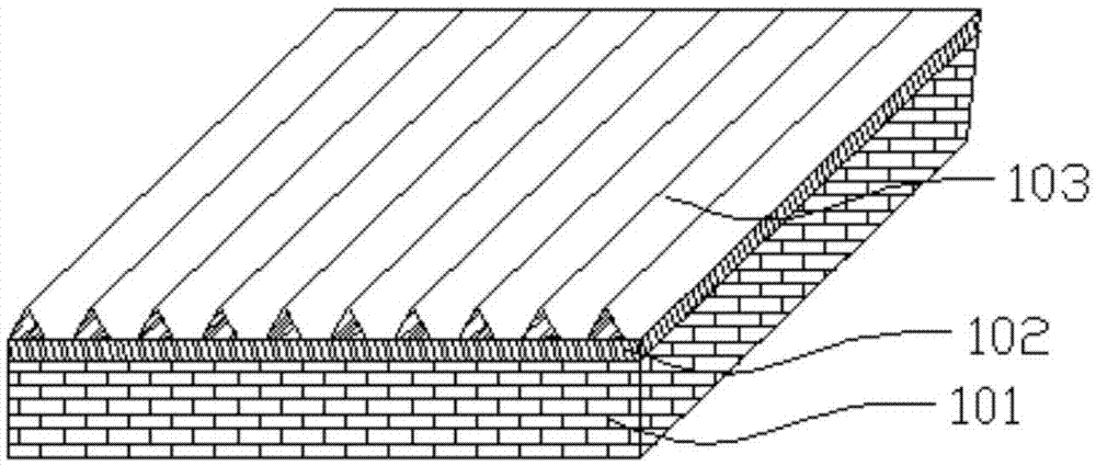
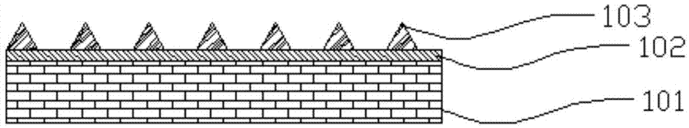
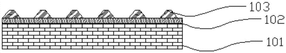
[0125] Step 1: Provide a composite graphic substrate 1 . Such as Figures 1 to 1 Growth substrates of several different structures shown in -4, this embodiment adopts fi...


PUM


Abstract

The invention relates to a flip-chip LED device with wafer-level packaging, a segmentation unit and a manufacturing method thereof. The flip-chip LED device comprises a flip-chip LED chip wafer / array including more than one LED chip, a conductive substrate and a phosphor transparent substrate. A metal layer a is formed at one side of the conductive substrate and is boned with electrode metals of the LED chips and a metal layer b is formed at the other side to form electrodes of the LED device. The conductive substrate is provided with a straight slot to isolate the electrodes of the LED device from each other. And the phosphor transparent substrate is combined with light-emitting surfaces, with growing substrates peeled, of the LED chips. According to the LED device, because of peeling of the growing substrates, the luminous efficiency of light at the chip and the excitation efficiency of the fluorescent powder are improved; bluelight side leakage after packaging is reduced; and thus the performance of the device is improved. Moreover, electrodes are isolated by the straight slot, so that the tedious wiring and insulation setting is avoided, the high-efficiency film upside-down mounting can be realized, and the packaging cost can be reduced.

Description

technical field [0001] The invention relates to the field of semiconductor lighting, in particular to a wafer-level packaged flip-chip LED device, a division unit and a manufacturing method thereof. Background technique [0002] In recent years, LED (Light Emitting Diode) product lighting has developed rapidly. Compared with traditional light sources, LED has the advantages of long life, small size, energy saving, high efficiency, fast response, shock resistance, and no pollution. It is considered to be a "green lighting source" that can enter the field of general lighting. [0003] As a connecting link in the LED industry chain, LED product packaging plays a key role in the entire industry chain. For packaging, the key technology boils down to how to extract as much light as possible from the chip within a limited cost range, while reducing the thermal resistance of the package and improving reliability. In the packaging process, packaging materials and packaging methods ...

Claims


Application Information

Patent Timeline
Patent Type & Authority Applications(China)
IPC IPC(8): H01L33/62H01L33/50
CPCH01L33/507H01L33/62H01L2933/0041H01L2933/0066
Inventor 郝茂盛张楠袁根如
Owner SHANGHAI XINYUANJI SEMICON TECH
Why Eureka
Try Eureka