
Optical proximity correction method

A technology of optical proximity effect and graphics, which is applied in optics, originals for photomechanical processing, instruments, etc., can solve the problems of long time and low correction efficiency of optical proximity effect correction, shorten the time used, and reduce the number of corrections , Improve the effect of correction efficiency

Active Publication Date: 2017-06-20
SEMICON MFG INT (SHANGHAI) CORP
View PDF5 Cites 4 Cited by
  • Summary
  • Abstract
  • Description
  • Claims
  • Application Information

AI Technical Summary

Problems solved by technology

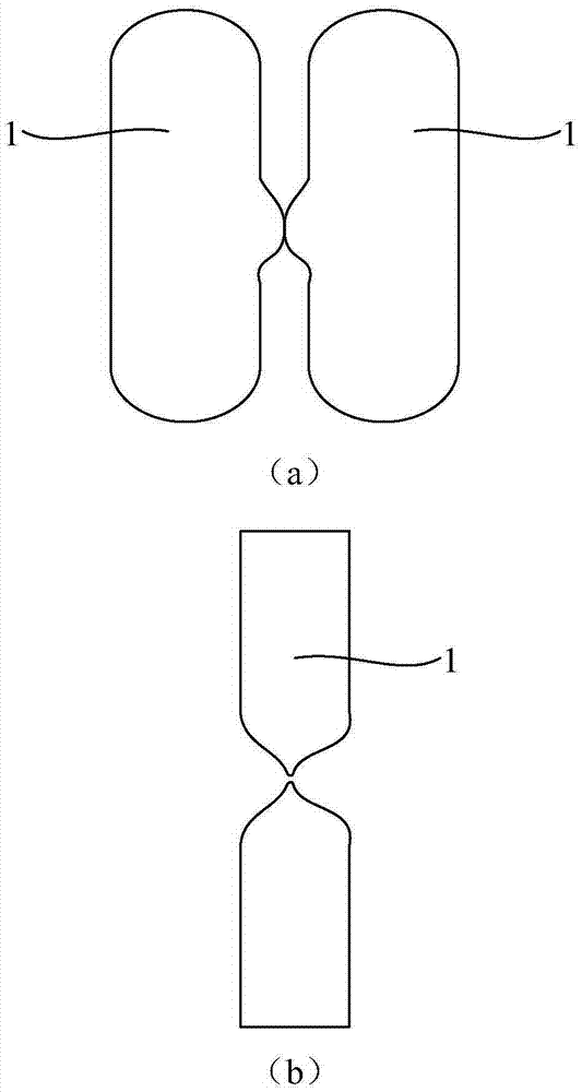
[0005] In the process of correcting the optical proximity effect, it is necessary to correct all the problem graphics to be corrected on the design layout one by one, so when there are N problem graphics to be corrected on the design layout, N times of correction are required, resulting in the correction of the optical proximity effect It takes too long and the correction efficiency is low

Method used


Image

  • Optical proximity correction method
  • Optical proximity correction method
  • Optical proximity correction method

Examples


Embodiment Construction

[0039] As mentioned above, in the existing optical proximity effect correction method, it is necessary to correct all the problem graphics to be corrected on the design layout one by one, so when there are N problem graphics to be corrected on the design layout, N times of corrections are required, resulting in The optical proximity effect correction takes too long and the correction efficiency is low.

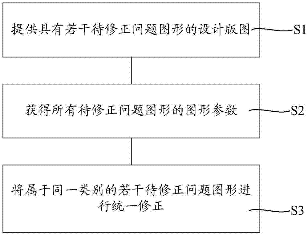
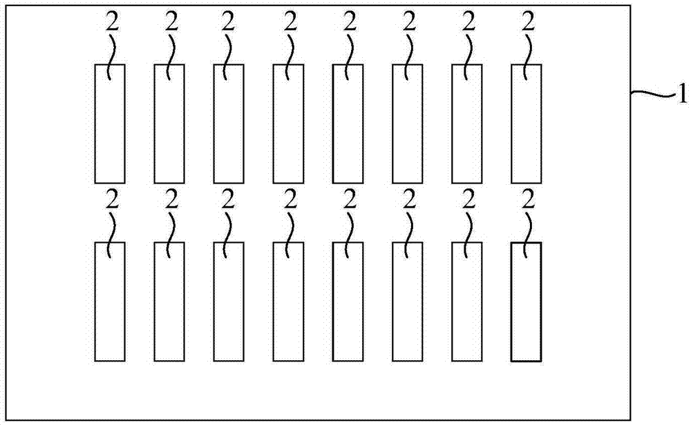
[0040] Considering that some of the problem graphics to be corrected in all the problem graphics to be corrected on some design layouts belong to the same category, and the principle that the problem graphics to be corrected belonging to the same category can be uniformly corrected in the same step, in the optical In the correction method of proximity effect, a number of problem graphics to be corrected belonging to the same category on the design layout are uniformly corrected in the same step, which avoids the correction of several problem graphics to be corrected in the same...


PUM


Abstract

The invention discloses an optical proximity correction method. The optical proximity correction method comprises the steps of providing a design layout of an integrated circuit, wherein the design layout comprises a plurality of to-be-corrected faulty graphs; measuring graph parameters of all the to-be-corrected faulty graphs; and performing unified correction on a plurality of to-be-corrected faulty graphs of the same category in all the to-be-corrected faulty graphs in the same step according to the graph parameters of all the to-be-corrected faulty graphs. According to the technical scheme of the invention, the multiple to-be-corrected faulty graphs of the same category in all the to-be-corrected faulty graphs are subjected to unified correction in the same step, so that correction on the to-be-corrected faulty graphs of the same category one by one is avoided; and therefore, the number of correction times of the to-be-corrected faulty graphs is reduced, optical proximity correction time is shortened, and correction efficiency is improved.

Description

technical field [0001] The invention relates to the technical field of semiconductors, in particular to an optical proximity effect correction method. Background technique [0002] In the semiconductor manufacturing process, the photolithography process is one of the most important process steps in the production of integrated circuits. With the development of semiconductor manufacturing technology, the feature size is getting smaller and smaller, and the requirements for resolution in the photolithography process are getting higher and higher. Lithography resolution refers to the minimum feature size (Critical Dimension, CD for short) that can be exposed on the surface of a silicon wafer by a lithography machine, and is one of the important performance indicators in lithography technology. [0003] However, with the development of semiconductor technology, the feature size of semiconductor devices is getting smaller and smaller. When the feature size is close to or even sm...

Claims


Application Information

Patent Timeline
Patent Type & Authority Applications(China)
IPC IPC(8): G03F1/36
CPCG03F1/36
Inventor 舒强
Owner SEMICON MFG INT (SHANGHAI) CORP
Learn More