Thin film transistor and manufacturing method

A technology of thin film transistors and etching grooves, which is applied in the fields of semiconductor/solid-state device manufacturing, semiconductor devices, electric solid-state devices, etc., can solve the problems of cumbersome preparation methods, low production efficiency, and many steps, etc.

Active Publication Date: 2019-11-08
TRULY HUIZHOU SMART DISPLAY
View PDF4 Cites 0 Cited by
  • Summary
  • Abstract
  • Description
  • Claims
  • Application Information

AI Technical Summary

Problems solved by technology

But this preparation method is more loaded down with trivial details, and steps are many, and production efficiency is lower.

Method used


Image

  • Thin film transistor and manufacturing method
  • Thin film transistor and manufacturing method
  • Thin film transistor and manufacturing method

Examples


Embodiment Construction

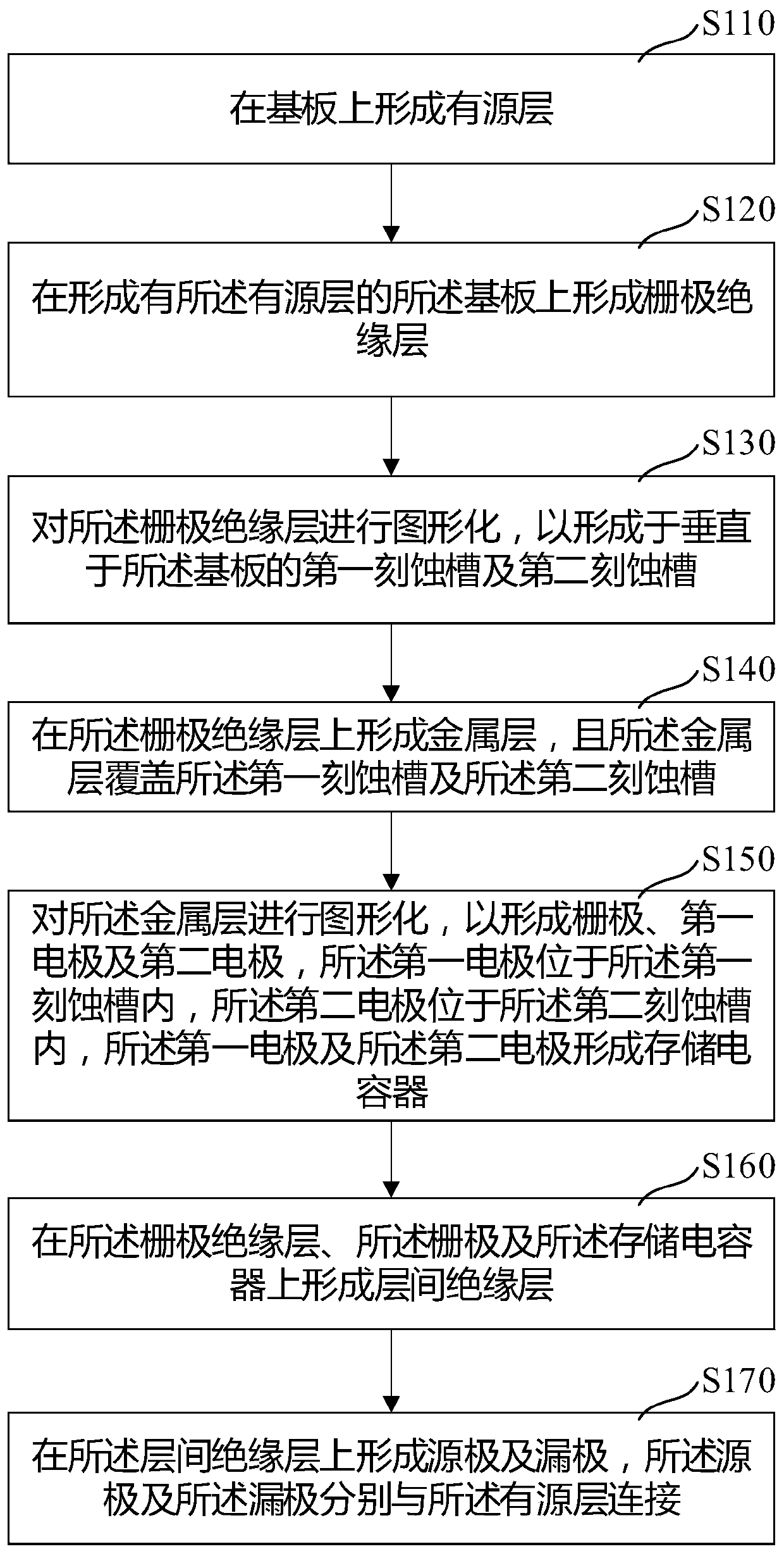
[0031] In order to make the above objects, features and advantages of the present invention more comprehensible, specific implementations of the present invention will be described in detail below in conjunction with the accompanying drawings. In the following description, numerous specific details are set forth in order to provide a thorough understanding of the present invention. However, the present invention can be implemented in many other ways different from those described here, and those skilled in the art can make similar improvements without departing from the connotation of the present invention, so the present invention is not limited by the specific embodiments disclosed below.

[0032] In describing the present invention, it should be understood that the terms "transverse", "length", "width", "thickness", "upper", "lower", "front", "rear", "left", " The orientation or positional relationship indicated by "right", "vertical", "horizontal", "top", "bottom", "inner"...


PUM


Abstract

The invention relates to a preparation method for a thin-film transistor. The preparation method comprises: an active layer is formed on a substrate; a gate insulating layer is formed on the substrate with the active layer; graphical processing is carried out on the gate insulating layer to form a first etching trench and a second etching trench that are perpendicular to the substrate; a metal layer is formed on the gate insulating layer and the metal layer covers the first etching trench and the second etching trench; graphical processing is carried out on the meta layer to form a first electrode and a second electrode and the first electrode and the second electrode form a storage capacitor; an interlayer insulation layer is formed on the gate insulating layer, a gate, and the storage capacitor; and a source electrode and a drain electrode are formed at the interlayer insulation layer and are connected with the active layer. The preparation method has advantages of simple process and high production efficiency. Moreover, because the first electrode and the second electrode are perpendicular to the substrate, the possibility of shielding by the electrode can be reduced, the aperture opening ratio of the thin-film transistor can be increased, and the capacity of the storage capacitor of the thin-film transistor can be enhanced.

Description

technical field [0001] The invention relates to the technical field of semiconductors, in particular to a thin film transistor and a preparation method. Background technique [0002] AMOLED, Active-Matrix Organic Light Emitting Diode (Active-Matrix Organic Light Emitting Diode), has been widely used because of its wide color gamut, high contrast, thinness, and low energy consumption, and is known as the next-generation display technology. [0003] With the development of display technology, Thin Film Transistor Liquid Crystal Display (TFT-LCD for short) has become the most common display device. In an AMOLED liquid crystal display, each sub-pixel is equipped with a thin film transistor, so that each sub-pixel Pixels can operate independently and are not easily affected by other sub-pixels. [0004] TFTs generally include storage capacitors. The storage capacitor includes a first electrode and a second electrode arranged in parallel. At present, in the manufacturing proces...

Claims


Application Information

Patent Timeline
Patent Type & Authority Patents(China)
IPC IPC(8): H01L27/12H01L21/77
CPCH01L27/1255H01L27/1259
Inventor 田金鹏张毅先任思雨苏君海李建华
Owner TRULY HUIZHOU SMART DISPLAY
Why Eureka
Try Eureka