A graphene-porous silicon material with high photoluminescence performance and preparation method thereof

A technology of porous silicon and graphene, applied in related application fields, can solve the problem of low photoluminescence performance of porous silicon, and achieve the effect of broadening optical application prospects, short time, and simple and easy steps

Active Publication Date: 2019-03-05
JIANGSU UNIV
View PDF3 Cites 0 Cited by
  • Summary
  • Abstract
  • Description
  • Claims
  • Application Information

AI Technical Summary

Problems solved by technology

The technical solution adopted by the present invention to solve the problem of the low photoluminescent performance of porous silicon is:

Method used


Image

  • A graphene-porous silicon material with high photoluminescence performance and preparation method thereof
  • A graphene-porous silicon material with high photoluminescence performance and preparation method thereof
  • A graphene-porous silicon material with high photoluminescence performance and preparation method thereof

Examples


Embodiment 1

[0032] 1. Select material: select the resistance of 3 ~ 8Ω.cm 2 1. An n-type monocrystalline silicon wafer (both sides polished) with a thickness of 450 μm and a crystal orientation of [100], with a size of 1.6 cm×1.6 cm.

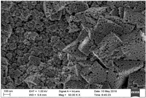
[0033] 2. Preparation of porous silicon: The above-mentioned selected samples were ultrasonically cleaned in absolute ethanol and deionized water for 20 minutes in sequence. Then remove it with tweezers and dry it with a nitrogen gun for later use. The prepared silicon wafer was electrochemically etched in a mixed solution of hydrofluoric acid / absolute ethanol with a volume ratio of 1:1, the current was set to 10mA, and the etching time was 10 minutes. After the etching was completed, it was cleaned with deionized water and washed with Blow dry with a nitrogen gun, such as figure 2 shown.

[0034] 3. Transfer of graphene: Cut the copper foil covered with graphene so that its size is equivalent to the size of the porous silicon. After the cutting is comp...

Embodiment 2

[0037] 1. Select material: select the resistance of 3 ~ 8Ω.cm 2 1. An n-type monocrystalline silicon wafer (both sides polished) with a thickness of 450 μm and a crystal orientation of [100], with a size of 1.6 cm×1.6 cm.

[0038] 2. Preparation of porous silicon: The above-mentioned selected samples were ultrasonically cleaned in absolute ethanol and deionized water for 20 minutes in sequence. Then remove it with tweezers and dry it with a nitrogen gun for later use. The prepared silicon wafer was electrochemically etched in a mixed solution of hydrofluoric acid / absolute ethanol with a volume ratio of 1:1, the current was set to 30mA, and the etching time was 10 minutes. After the etching was completed, it was cleaned with deionized water and washed with Blow dry with a nitrogen gun.

[0039] 3. Transfer of graphene: Cut the copper foil covered with graphene so that its size is equivalent to the size of the porous silicon. After the cutting is completed, place the copper fo...

Embodiment 3

[0041] 1. Select material: select the resistance of 3 ~ 8Ω.cm 2 1. An n-type monocrystalline silicon wafer (both sides polished) with a thickness of 450 μm and a crystal orientation of [100], with a size of 1.6 cm×1.6 cm.

[0042]2. Preparation of porous silicon: The above-mentioned selected samples were ultrasonically cleaned in absolute ethanol and deionized water for 20 minutes in sequence. Then remove it with tweezers and dry it with a nitrogen gun for later use. The prepared silicon wafers were electrochemically etched in a mixed solution of hydrofluoric acid / absolute ethanol with a volume ratio of 1:1, the current was set to 30mA, and the time was 10 minutes. After the etching was completed, it was cleaned with deionized water and nitrogen gas Gun blow dry.

[0043] 3. Transfer of graphene: Cut the copper foil covered with graphene so that its size is equivalent to the size of the porous silicon. After the cutting is completed, place the copper foil on the glass sheet,...


PUM

PropertyMeasurementUnit
thicknessaaaaaaaaaa

Abstract

The invention provides a graphene-porous silicon material having high photoluminescence property and a preparation method. The preparation method comprises the following steps: 1, preparing a single layer of graphene on a copper foil by using a CVD method to obtain the copper foil covered by the graphene; 2, selecting an n-type monocrystalline silicon wafer, and polishing the two surfaces thereof; 3, performing a ultrasonic cleaning on the n-type monocrystalline silicon wafer, treated in step 2, sequentially in absolute ethyl alcohol and deionized water, and then blow-drying; electrochemically corroding the blow-dried n-type monocrystalline silicon wafer in a hydrofluoric acid / absolute ethyl alcohol mixed solution; and cleaning with deionized water after the electrochemical corrosion is finished, and blow-drying to obtain a porous silicon; 4, after the graphene is treated, recombinating the surface of the porous silicon and the graphene; and finally, putting the graphene-porous silicon composite material into acetone for degumming to obtain the graphene-porous silicon material having high photoluminescence property. The graphene-porous silicon material prepared in the invention has advantages that the optical property index of the porous silicon is obviously improved and the optical application prospect of the porous silicon is widened.

Description

technical field [0001] The present invention relates to related application fields of nanoporous silicon materials such as luminescent properties, luminescent materials, and luminescent devices. The invention is a graphene-porous silicon material with high photoluminescence performance and a preparation method thereof. Background technique [0002] Porous Silicon is a porous silicon material with nanostructure formed by electrochemical corrosion of silicon wafers. Porous silicon has high resistivity, large specific surface area and high chemical activity, and new progress has been made in the luminescence of porous silicon. However, porous silicon has always had the problem of low luminous efficiency. How to improve the photoluminescence properties of porous silicon has become one of the problems that people pay close attention to urgently. In order to overcome this shortcoming, people have tried various methods, by performing pulse treatment on the surface of single crys...

Claims


Application Information

Patent Timeline
Patent Type & Authority Patents(China)
IPC IPC(8): C09K11/02C09K11/59C23C16/26C25F3/12
CPCC09K11/025C09K11/59C23C16/26C25F3/12
Inventor 葛道晗张立强钱栋梁程广贵丁建宁
Owner JIANGSU UNIV
Why Eureka
Try Eureka