LED wafer dead pixel picking sorting method

A technology of dead pixels and wafers, which is applied in the field of sorting LED wafers, can solve the problems of consuming sorting machine capacity, loss of qualified chips, large manpower and production time, etc., to improve the removal rate of dead pixels and The effect of success rate, capacity saving and manpower saving

Inactive Publication Date: 2017-06-27
FOCUS LIGHTINGS SCI & TECH
View PDF6 Cites 10 Cited by
  • Summary
  • Abstract
  • Description
  • Claims
  • Application Information

AI Technical Summary

Problems solved by technology

[0003] At present, LED chip manufacturers are basically similar to the production method of square chips in providing bad point wafers. First, the testing machine tests all the chip data on the chip source, and then the sorting machine sorts out the unsuitable (NG) chips. The core particles are picked out one by one, and the remaining ones after the removal are the bad point wafers. The process of removing bad points will inevitably consume a lot of capacity of the sorting machine, and it will also take up a lot of manpower and production time. In addition, the sorting The machine also has the action of image recognition and mechanical point suction. There is a certain phenomenon of aspiration and leakage in the whole process, resulting in the loss of some qualified chips and the existence of bad pixels that cannot be removed. The existence of bad pixels may even cause customer complaints.

Method used


Image

  • LED wafer dead pixel picking sorting method
  • LED wafer dead pixel picking sorting method
  • LED wafer dead pixel picking sorting method

Examples


Embodiment Construction

[0029] In order to enable those skilled in the art to better understand the technical solutions of the present invention, the present invention will be described in detail below in conjunction with specific implementations shown in the accompanying drawings. However, these embodiments do not limit the present invention, and any structural, method, or functional changes made by those skilled in the art according to these embodiments are included in the protection scope of the present invention.

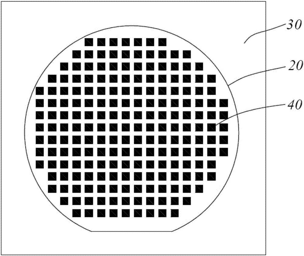
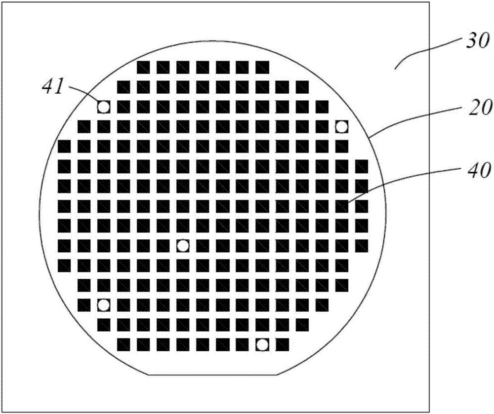
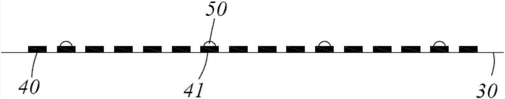
[0030] Preferred embodiments of the present invention, such as figure 1 As shown, a wafer 20 to be tested to pick out bad spots is provided. The wafer 20 here refers to a large wafer that has been cut, that is, a wafer (wafer). The wafer becomes a semiconductor grain after epitaxy and cutting. It is the most commonly used semiconductor material, divided into 4 inches, 5 inches, 6 inches, 8 inches, 12 inches, 14 inches, 15 inches, 16 inches, ... 20 inches and above according to its diam...


PUM


Abstract

The invention discloses an LED wafer dead pixel picking sorting method. The method comprises the following steps that (1) a to-be-tested wafer for dead pixel picking is provided; (2) core grains on the wafer are tested one by one; (3) crystal grains proven to be dead pixels through testing results are marked; (4) a film is attached to the surface of the wafer, and the dead pixel crystal grains are bonded with the film through marks; and (5) the film is torn down so that the dead pixel crystal grains can be separated from the wafer. According to the LED dead pixel picking wafer sorting method, the dead pixels on the wafer are removed at a time by bonding the film with the dead pixel crystal grains, the dead pixel removal rate and success rate are greatly increased, operation is simple and convenient, and manpower is saved.

Description

technical field [0001] The invention relates to the technical field of LED semiconductors, in particular to a method for sorting bad spots of LED wafers. Background technique [0002] There are usually two ways to ship chips in the LED market, 1: square chip shipments; 2: round chip shipments, where the wafers are subdivided into large wafers and single-defect wafers. The so-called square chip refers to the testing and sorting of LED chips according to the photoelectric characteristics such as wavelength, luminous intensity, and working voltage. The source is handed over to the sorting machine to automatically pack the LED chips into different types of output boxes (BIN boxes) according to the set standards, so that the sorted chips are called square chips. As the LED upstream and downstream industry chains have higher and higher requirements for cost reduction, the continuous upgrading and maturity of the epitaxial wafer production process and conditions, and the continuou...

Claims


Application Information

Patent Timeline
Patent Type & Authority Applications(China)
IPC IPC(8): B07C5/344B07C5/342B07C5/36
Inventor 张广庚陈立人李庆
Owner FOCUS LIGHTINGS SCI & TECH
Why Eureka
Try Eureka