
Touch electronic equipment, touch display device and array substrate gate drive circuit

A technology of gate drive circuit and array substrate, applied in static indicators, electrical digital data processing, digital memory information, etc., can solve the problem of insufficient charging of TFT in the pixel area, achieve good touch display effect, and ensure touch display Effects, fast-response effects

Active Publication Date: 2019-08-02
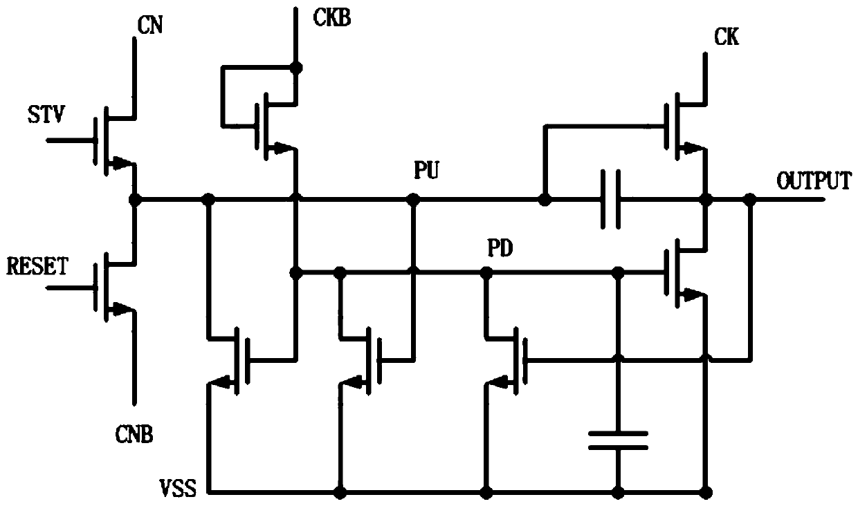
BOE TECH GRP CO LTD +1
View PDF4 Cites 0 Cited by
  • Summary
  • Abstract
  • Description
  • Claims
  • Application Information

AI Technical Summary

Problems solved by technology

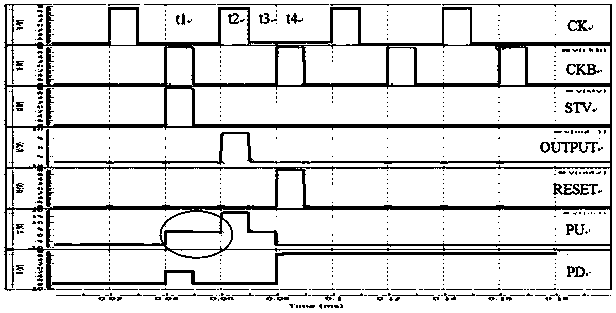
For this reason, the first object of the present invention is to propose an array substrate gate drive circuit, which can effectively increase the PU node level of the GOA at the level that needs to be started after the touch function of the display panel, thereby solving the problem of Insufficient charging of TFT in the pixel area

Method used


Image

  • Touch electronic equipment, touch display device and array substrate gate drive circuit
  • Touch electronic equipment, touch display device and array substrate gate drive circuit
  • Touch electronic equipment, touch display device and array substrate gate drive circuit

Examples


Embodiment Construction

[0026] Embodiments of the present invention are described in detail below, examples of which are shown in the drawings, wherein the same or similar reference numerals designate the same or similar elements or elements having the same or similar functions throughout. The embodiments described below by referring to the figures are exemplary and are intended to explain the present invention and should not be construed as limiting the present invention.

[0027] The array substrate gate drive circuit, touch display device and touch electronic equipment according to the embodiments of the present invention will be described below with reference to the accompanying drawings.

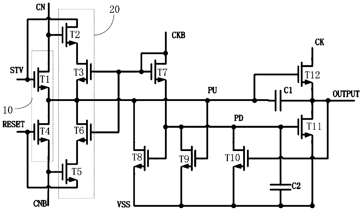
[0028] As shown in the accompanying drawings, the array substrate gate driving circuit proposed by the embodiment of the present invention includes: a first capacitor C1 , a charging path 10 and a charging and discharging path 20 .

[0029] like figure 2 As shown, one end of the first capacitor C1 is used as...


PUM


Abstract

The embodiments of the present disclosure relate to a shift registers unit and a driving method thereof, and a gate driving device. The shift register unit includes a first and second input circuit, a pull-down control circuit, an output circuit, a pull-down circuit, and a control circuit. The first input circuit provides a first control signal to a pull-up node. The second input circuit provides a second control signal to the pull-up node. The pull-down control circuit provides the voltage of a first voltage terminal to a pull-down node, or controls the voltage of the pull-down node. The output circuit provides a second clock signal to a signal output terminal. The pull-down circuit provides the voltage of the first voltage terminal to the pull-up node and the signal output terminal. The control circuit provides the first input signal to the pull-up node.

Description

technical field [0001] The present invention relates to the field of display control technology, in particular to an array substrate gate drive circuit, a touch display device and a touch electronic device. Background technique [0002] Display panel with Touch (touch) function, Display (display) and Touch are time-division multiplexed. After the Touch is over, the GOA (Gate Driver on Array, array substrate gate drive) of the level that needs to be started remains at a high level during the Touch phase PU (Pull Up, pull-up) node, because the PU node will leak electricity, causing the Touch After the end, the level of the PU node of the GOA that needs to be started is low, so the TFT (Thin Film Transistor, Thin Film Transistor) in the pixel area is insufficiently charged, which affects the display touch effect. Contents of the invention [0003] This application is based on the inventor's understanding and research on the following issues: [0004] The GOA circuit of 8T2C...

Claims


Application Information

Patent Timeline
Patent Type & Authority Patents(China)
IPC IPC(8): G06F3/041G09G3/20
CPCG06F3/0416G09G3/20G09G3/3266G09G3/3677G09G2300/0408G09G2310/0286G11C19/28
Inventor 王珍孙建乔赟詹小舟黄飞张寒秦文文丛乐乐王争奎
Owner BOE TECH GRP CO LTD
Learn More