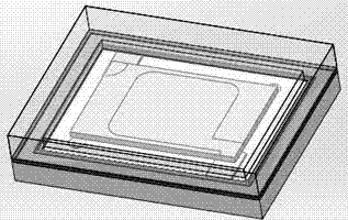
Full ceramic adhesive bonding packaging technology applied to crystal resonator
A crystal resonator and packaging process technology, applied in electrical components, impedance networks, etc., can solve problems such as high production costs, increased supply risks, shortages, etc., to achieve high air tightness, avoid high production costs, adhesive good effect
- Summary
- Abstract
- Description
- Claims
- Application Information
AI Technical Summary
Problems solved by technology
Method used
Image
Examples
Embodiment Construction
[0020] An all-ceramic adhesive bonding packaging process applied to crystal resonators, characterized in that it comprises the following steps:
[0021] 1) Production of ceramic base: select blank ceramic sheets, use a laser drilling machine to punch holes in the ceramic sheets line by line, grind the ceramic sheets with micro-through holes, and clean the holes left on the back of the ceramic sheets after laser slag, and ultrasonically clean and dry the ceramic sheet, pour conductive paste into the micro through hole of the ceramic sheet, put it in an oven to solidify, and form an electronic circuit channel, and then use screen printing to print the circuit on the front and back of the ceramic sheet , and sintered in 5 temperature zones in the sintering furnace to form metal dispensing pads and metal pads, and finally use a laser slicer to scribe the circuitized ceramic sheets, and divide the large electric polarized ceramic sheets into Small pieces, washed and dried to obtain...
PUM
 Abstract
Description
Claims
Application Information


