Adhesive pad, display panel, display device and electrostatic protection method thereof

A technology for a display panel and a display device, applied in the fields of display device and its electrostatic protection, bonding pad, and display panel, can solve the problems of complicated manufacturing process, the bonding pad is easily attacked by static electricity, destroying the display panel, etc. rate effect

Active Publication Date: 2020-07-03
WUHAN CHINA STAR OPTOELECTRONICS TECH CO LTD
View PDF5 Cites 0 Cited by
  • Summary
  • Abstract
  • Description
  • Claims
  • Application Information

AI Technical Summary

Problems solved by technology

The manufacturing process of the LTPS panel is complicated. During the manufacturing process, the bonding pads on the edge of the panel are easily attacked by static electricity. Through the conductive effect of the bonding pads, the display pixel units on the panel are also attacked by static electricity, destroying the entire display panel. Therefore, enhancing LTPS The antistatic function of the panel is of great significance for improving the yield rate of the display panel and reducing the manufacturing cost of the panel

Method used


Image

  • Adhesive pad, display panel, display device and electrostatic protection method thereof
  • Adhesive pad, display panel, display device and electrostatic protection method thereof
  • Adhesive pad, display panel, display device and electrostatic protection method thereof

Examples


Embodiment Construction

[0036] In order for those skilled in the art to better understand the technical solution of the present invention, an adhesive pad, a display panel, a display device and an electrostatic protection method thereof provided by the present invention will be further described in detail below with reference to the accompanying drawings and specific embodiments. In the drawings, the same reference numerals are used to denote the same structures and regions throughout the specification and drawings.

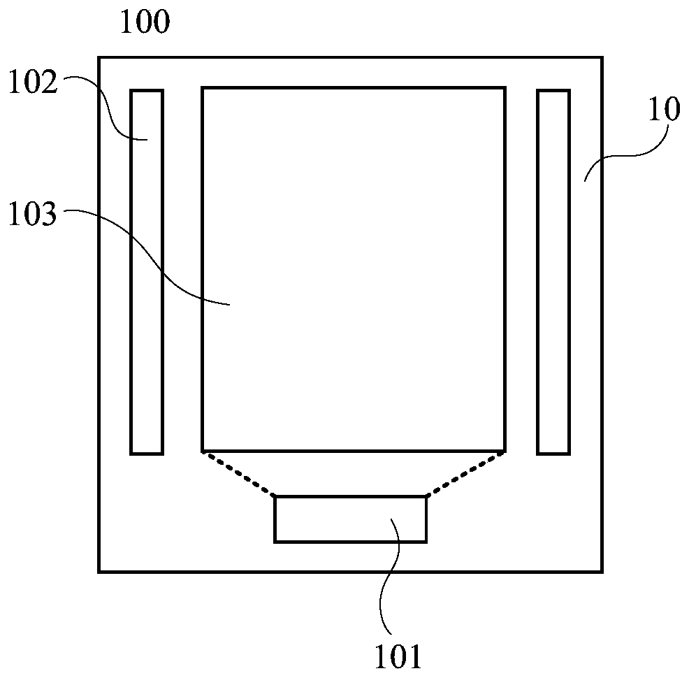
[0037] refer to figure 1 , figure 1 It is a structural schematic diagram of a display panel in the prior art. Such as figure 1 As shown, the display panel 100 includes a display area and a non-display area, the display area is provided with a display pixel unit 103, the non-display area on both sides of the display area is used to set the GOA driving circuit 102, and the other side of the display area is provided with a bonding area The bonding area is provided with a plurality of bo...


PUM


Abstract

The invention discloses a bonding pad, a display panel, a display device and an electrostatic protection method. The bonding pad is sequentially divided into a first area and a second area from the edge of the display panel to the center of the display panel, a first polysilicon conductive layer is arranged between the first area and the second area, and the first area and the second area are electrically connected through the first polysilicon conductive layer. When the bonding pad is subjected to an electrostatic shock, a corresponding electrostatic current will be transmitted to the second area from the first area and will cause the fusion of the first polysilicon conductive layer, the electrostatic current between the first area and the second area is cut off, and then, a display pixel unit of the display panel is protected, so that the yield rate of manufacturing of the display panel is increased.

Description

technical field [0001] The invention relates to the technical field of liquid crystal display panels, in particular to an adhesive pad, a display panel, a display device and an electrostatic protection method thereof. Background technique [0002] Due to the continuous improvement of device integration and circuit density, the breakdown voltage is getting lower and lower. Static electricity is known as the "invisible enemy" in the electronics industry. Therefore, the protection of static electricity is mainly devoted to prevent problems before they happen, and carry out comprehensive protection against ESD (Electro-Static discharge, electrostatic discharge). [0003] At present, LTPS (Low Temperature Poly-silicon, low-temperature polysilicon) panels have been widely used in smart terminals, and many types of smart phones and tablet computers on the market use LTPS panels. The manufacturing process of the LTPS panel is complicated. During the manufacturing process, the bond...

Claims


Application Information

Patent Timeline
Patent Type & Authority Patents(China)
IPC IPC(8): G02F1/1345
CPCG02F1/13452
Inventor 虞晓江
Owner WUHAN CHINA STAR OPTOELECTRONICS TECH CO LTD
Why Eureka
Try Eureka