Display panel, display device and driving method of pixel circuit

A display panel and pixel circuit technology, applied in the computer field, can solve problems such as uneven display

Active Publication Date: 2017-06-30
WUHAN TIANMA MICRO ELECTRONICS CO LTD
View PDF6 Cites 76 Cited by
  • Summary
  • Abstract
  • Description
  • Claims
  • Application Information

AI Technical Summary

Problems solved by technology

[0005] In view of this, an embodiment of the present invention provides a display panel, a display device, and a driving method for a pixel circuit to solve the problem of uneven display in the prior art

Method used


Image

  • Display panel, display device and driving method of pixel circuit
  • Display panel, display device and driving method of pixel circuit
  • Display panel, display device and driving method of pixel circuit

Examples


Embodiment 1

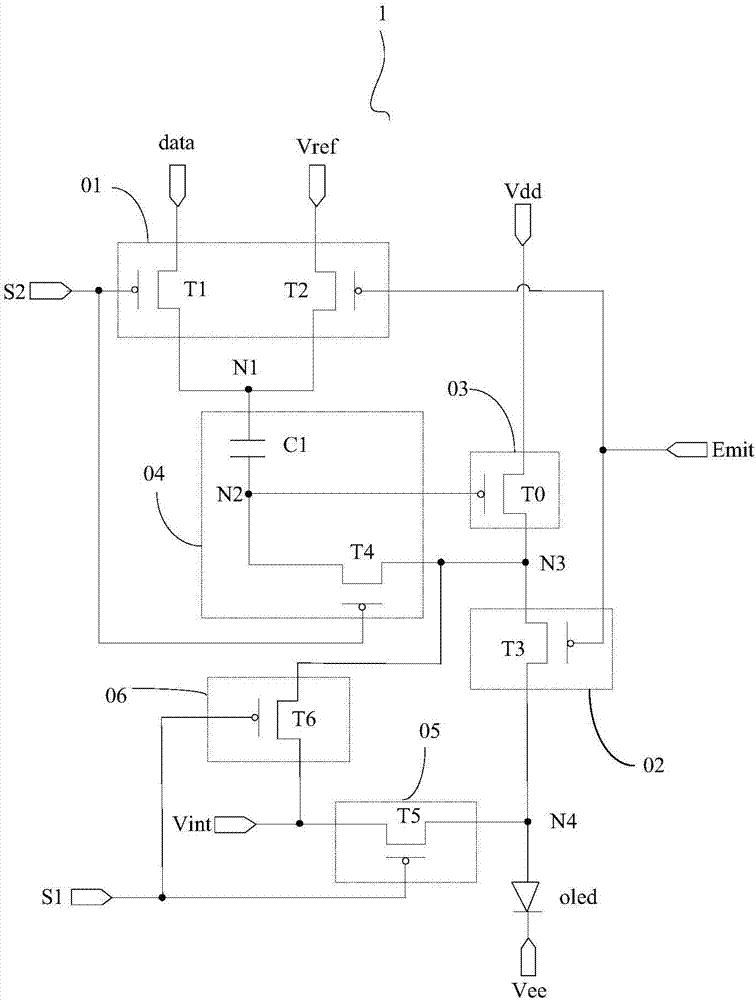
[0058] Figure 3a , Figure 4a and Figure 5a The timing corresponding to the pixel circuit shown is as follows Figure 6a When shown, it includes three stages t1, t2 and t3.

[0059] In the t1 stage, S1=0, S2=0, Emit=1.

[0060] The first transistor T1 , the fourth transistor T4 , the fifth transistor T5 , the sixth transistor T6 and the driving transistor T0 are turned on, and the second transistor T2 and the third transistor T3 are turned off. The potential of the first node N1 is the potential Vdata on the data line data, the second node N2=Vint, the third node N3=Vint, the fourth node N4=Vint, and the light emitting diode oled does not emit light. That is, the functions of node initialization and anode reset of the light-emitting diode oled are realized in the t1 stage.

[0061] In the t2 stage, S1=1, S2=0, Emit=1.

[0062] The first transistor T1, the fourth transistor T4 and the driving transistor T0 are turned on, and the second transistor T2, the third transisto...

Embodiment 2

[0066] Figure 3a , Figure 4a and Figure 5a The timing corresponding to the pixel circuit shown is as follows Figure 6b When shown, four stages including t0, t1, t2 and t3 are included.

[0067] At stage t0, S1=0, S2=1, Emit=1.

[0068] The fifth transistor T5 and the sixth transistor T6 are turned on, and the driving transistor T0 , the first transistor T1 , the second transistor T2 , the third transistor T3 and the fourth transistor T4 are turned off. The fourth node N4=Vint, the potential of the node connected to the second pole of the sixth transistor T6 is Vint, and the light emitting diode oled does not emit light. That is, the functions of node initialization and anode reset of the light-emitting diode oled are realized in the t0 stage.

[0069] In the t1 stage, S1=0, S2=0, Emit=1.

[0070]The first transistor T1 , the fourth transistor T4 , the fifth transistor T5 , the sixth transistor T6 and the driving transistor T0 are turned on, and the second transistor ...

Embodiment 3

[0077] Figure 3b , Figure 4b and Figure 5b The timing corresponding to the pixel circuit shown is as follows Figure 6a When shown, it includes three stages t1, t2 and t3.

[0078] In the t1 stage, S1=0, S2=0, Emit=1.

[0079] The first transistor T1 , the fourth transistor T4 , the fifth transistor T5 , the sixth transistor T6 and the driving transistor T0 are turned on, and the second transistor T2 and the third transistor T3 are turned off. The potential of the first node N1 is the potential Vdata on the data line data, the second node N2=Vint, the third node N3=Vint, the fourth node N4=Vint, and the light emitting diode oled does not emit light. That is, the functions of node initialization and anode reset of the light-emitting diode oled are realized in the t1 stage.

[0080] In the t2 stage, S1=1, S2=0, Emit=1.

[0081] The first transistor T1, the fourth transistor T4, the fifth transistor T5 and the driving transistor T0 are turned on, and the second transisto...


PUM


Abstract

The invention discloses a display panel, a display device and a driving method of a pixel circuit. The pixel circuit comprises a data writing module, a light-emitting control module, a driving control module, a threshold compensation module, an anode reset module, a node initialization module and an organic light-emitting diode. The threshold compensation module can compensate the drift of threshold voltages of a driving transistor so that light-emitting working currents of a light-emitting device which is driven by the driving transistor are only related to signals of data cables and voltages of a reference signal end and not related to the threshold voltages and a first power supply voltage end, and the influence of the threshold voltages and IR Drop on currents which flow through the organic light-emitting diode can be avoided. Furthermore, the anode reset module can reset an anode potential of the organic light-emitting diode so that the organic light-emitting diode does not emit light completely in a dark state. In addition, an initial signal end and the reference signal end are set separately, not only can the problems of crosstalk and uneven display of the circuit be improved, but also the range of data signals can be increased.

Description

technical field [0001] The invention relates to the field of computer technology, in particular to a display panel, a display device and a driving method for a pixel circuit. Background technique [0002] Organic Light Emitting Diode (OLED) display is one of the hotspots in the field of flat panel display research today. Compared with liquid crystal display, OLED display has the advantages of low energy consumption, low production cost, self-illumination, wide viewing angle and fast response speed. Currently, OLED displays have begun to replace traditional Liquid Crystal Displays (LCDs) in the fields of flat panel displays such as mobile phones, PDAs, and digital cameras. Among them, pixel circuit design is the core technical content of OLED display, which has important research significance. [0003] Unlike LCD, which uses a stable voltage to control brightness, OLED is current-driven and requires a stable current to control light emission. Due to reasons such as process ...

Claims


Application Information

Patent Timeline
Patent Type & Authority Applications(China)
IPC IPC(8): G09G3/3233G09G3/3266
CPCG09G3/3233G09G3/3266G09G2320/0233G09G2300/0814G09G2300/0819G09G2300/0842G09G2300/0861G09G2310/0245G09G2310/0262G09G2320/0209G09G2330/02
Inventor 朱仁远陈泽源
Owner WUHAN TIANMA MICRO ELECTRONICS CO LTD
Why Eureka
Try Eureka