System-in-package multi-chip interconnection test method and system-in-package multi-chip interconnection test device

A system-level packaging and testing method technology, applied in the field of integrated circuits, can solve problems affecting the accuracy of SIP chips and the interconnection testing of various bare chips.

Inactive Publication Date: 2017-07-07
SANECHIPS TECH CO LTD
View PDF6 Cites 5 Cited by
  • Summary
  • Abstract
  • Description
  • Claims
  • Application Information

AI Technical Summary

Problems solved by technology

When testing SiP chips, traditional chip testing methods can only test each die independently to ensure the test results

Method used


Image

  • System-in-package multi-chip interconnection test method and system-in-package multi-chip interconnection test device
  • System-in-package multi-chip interconnection test method and system-in-package multi-chip interconnection test device
  • System-in-package multi-chip interconnection test method and system-in-package multi-chip interconnection test device

Examples


Embodiment Construction

[0039] The following will clearly and completely describe the technical solutions in the embodiments of the present invention with reference to the drawings in the embodiments of the present invention.

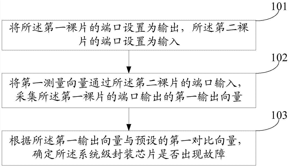
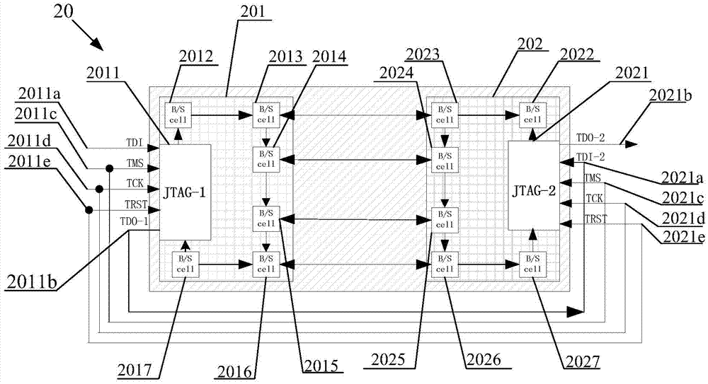
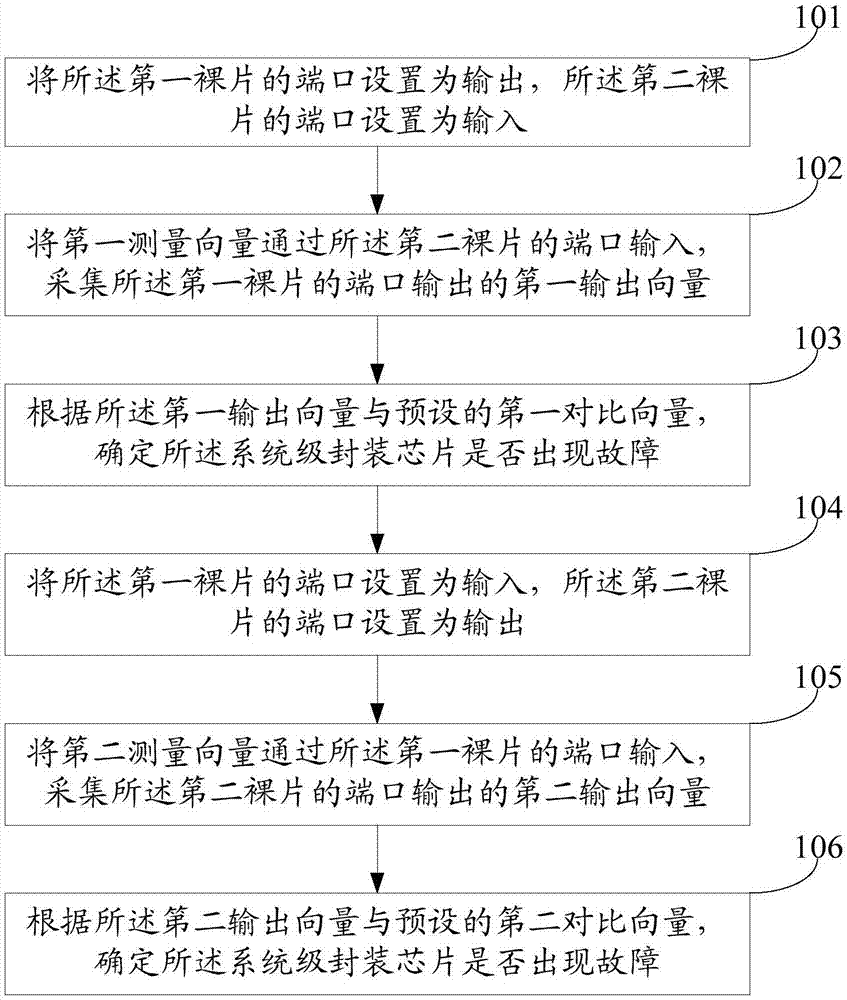
[0040] An embodiment of the present invention provides a system-in-package multi-chip interconnection testing method for a system-in-package chip, the system-in-package chip at least including a first die and a second die interconnected with the first die, Both the first die and the second die include a joint test working group JTAG interface, and the first die and the second die form a serial JTAG structure; the system-in-package chip can also be It is called a SIP chip. Such as figure 1 As shown, the system-in-package multi-chip interconnection testing method includes:

[0041] Step 101. Set the port of the first die as an output, and the port of the second die as an input.

[0042] example, such as figure 2 As shown, the system-in-package chip 20 may include a first di...


PUM


Abstract

The embodiment of the invention discloses a system-in-package multi-chip interconnection test method for a system-in-package chip. The system-in-package chip at least comprises a first bare die and a second bare die interconnected with the first bare die; each of the first bare die and the second bare die comprises a JTAG interface of a joint test work group; and the first bare die and the second bare die form a serial JTAG structure. The method comprises steps: the port of the first bare die is set to be output, and the port of the second bare die is set to be input; a first measurement vector is inputted through the port of the second bare die, and a first output vector outputted by the port of the first bare die is acquired; and according to the first output vector and a preset comparison vector, whether fault happens to the system-in-package chip is determined. Further, the embodiment of the invention also discloses a system-in-package multi-chip interconnection test device.

Description

technical field [0001] The invention relates to chip testing technology in the field of integrated circuits, in particular to a system-in-package multi-chip interconnection testing method and device. Background technique [0002] With the development of integrated circuits, chip packaging technology is increasingly pursuing miniaturization, multi-function and low cost, so SiP (System in Package, system-in-package) came into being. [0003] The SiP integrates chips with multiple functions, including chips such as processors and memories, into one package to realize a basically complete function. Compared with traditional independent packaging, SiP can maximize the integration of silicon chips and utilize the effective area of ​​silicon chips at the lowest cost; it can also reduce the electrical path length between chips, thereby improving device performance; in addition, SiP also allows heterogeneous integration, which can integrate analog circuits, digital circuits, RF and ...

Claims


Application Information

Patent Timeline
IPC IPC(8): G01R31/28
CPCG01R31/00G01R31/2803G01R31/2806
Inventor 刘军强
Owner SANECHIPS TECH CO LTD
Why Eureka
Try Eureka