Wafer scale micrometer-nanometer scale semiconductor LED display screen and preparation method thereof
A LED display screen and semiconductor technology, applied in the manufacture of semiconductor/solid-state devices, semiconductor devices, electric solid-state devices, etc., can solve the problems that the manufacturing process is difficult to extend, and the chip pixel size is difficult to further reduce, so as to achieve the convenience of the manufacturing process Effect
- Summary
- Abstract
- Description
- Claims
- Application Information
AI Technical Summary
Problems solved by technology
Method used
Image

Examples
Embodiment Construction
[0042] The following embodiments will further illustrate the present invention in conjunction with the accompanying drawings.
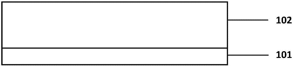
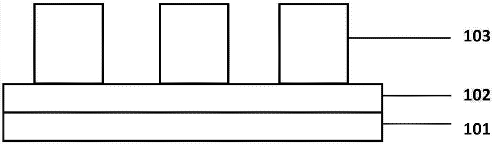
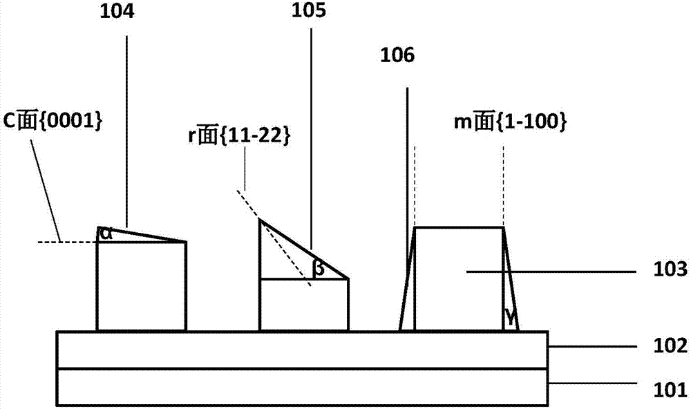
[0043] The embodiment of the wafer-level micro-nano-scale semiconductor LED display screen includes a first substrate, a first semiconductor layer, a second semiconductor layer, a third semiconductor layer, a transparent isolation layer and a transparent conductive layer, and the second semiconductor 3x groups of different surfaces are made respectively, and the 3x groups of different surfaces are the first group of surfaces with the angle α with the c-plane, the second group of surfaces with the angle β with the r-plane and the surface with the angle γ with the m-plane The third group of surfaces, the c-plane angle α, the r-plane angle β and the m-plane angle γ are: 0°x Ga 1-x N / GaN material; the first multi-quantum well active layer can obtain the red light R band with a wavelength of 580-680nm by controlling the crystal plane angle α, and the secon...
PUM
| Property | Measurement | Unit |
|---|---|---|
| Wavelength | aaaaa | aaaaa |
| Wavelength | aaaaa | aaaaa |
| Size | aaaaa | aaaaa |
Abstract
Description
Claims
Application Information
 - Generate Ideas
- Intellectual Property
- Life Sciences
- Materials
- Tech Scout
- Unparalleled Data Quality
- Higher Quality Content
- 60% Fewer Hallucinations
Browse by: Latest US Patents, China's latest patents, Technical Efficacy Thesaurus, Application Domain, Technology Topic, Popular Technical Reports.
© 2025 PatSnap. All rights reserved.Legal|Privacy policy|Modern Slavery Act Transparency Statement|Sitemap|About US| Contact US: help@patsnap.com