LED package device and packaging method thereof

A technology for LED packaging and LED devices, applied in semiconductor devices, electrical components, circuits, etc., can solve the problems of unsolved packaging glue and easy falling off, and achieve the effects of improving luminous flux, simple packaging operation and high efficiency

Pending Publication Date: 2017-07-14
SHENZHEN GUOYEXING OPTOELECTRONICS TECH CO LTD
View PDF13 Cites 2 Cited by
  • Summary
  • Abstract
  • Description
  • Claims
  • Application Information

AI Technical Summary

Problems solved by technology

However, this patent improves the bonding force between the white reflective plastic and the metal plate through the primer transition layer, thereby improving the high temperature and humidity resistance of the LED device, and does not solve the problem that the encapsulation glue is easy to fall off due to aging

Method used


Image

  • LED package device and packaging method thereof
  • LED package device and packaging method thereof

Examples


Embodiment 1

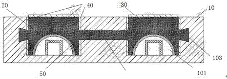
[0045] Such as figure 1 As shown, this embodiment provides an LED packaging device, including a substrate 10, a chip 20 and an encapsulation layer 30. There are two chips 20; the substrate 10 is provided with two mounting grooves 101, and the chip 20 is installed in the corresponding mounting groove 101 Inside, a through hole 102 is provided between adjacent mounting grooves 101; the packaging layer 30 fills the mounting groove 101 through the through hole 102, the packaging layer 30 covers the chip 20, and the upper surface of the packaging layer 30 is provided with a phosphor layer 40; the mounting groove 101 The side is provided with a groove 103, and the corresponding part of the packaging layer 30 is provided with a protrusion matching the shape of the groove 103; the groove 103 is a trapezoidal groove, and the upper surface of the trapezoidal groove is the opening end of the trapezoidal groove; the installation groove 101, the through hole 102 A reflection layer is provi...

Embodiment 2

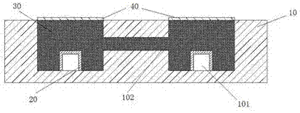
[0052] Such as figure 2 As shown, this embodiment provides an LED packaging device, including a substrate 10, a chip 20 and an encapsulation layer 30. There are two chips 20; the substrate 10 is provided with two mounting grooves 101, and the chip 20 is installed in the corresponding mounting groove 101 Inside, a through hole 102 is provided between adjacent mounting grooves 101 ; the encapsulation layer 30 fills the mounting groove 101 through the through hole 102 , the encapsulation layer 30 covers the chip 20 , and the upper surface of the encapsulation layer 30 is provided with a phosphor layer 40 .

Embodiment 3

[0054] This embodiment provides an LED packaging device, including a substrate 10, a chip 20 and an encapsulation layer 30. There are two chips 20; A through hole 102 is provided between the adjacent mounting grooves 101; the packaging layer 30 penetrates the through hole 102 and fills the mounting groove 101, the packaging layer 30 covers the chip 20, and the upper surface of the packaging layer 30 is provided with a phosphor layer 40; the inner wall of the mounting groove 101 is rough noodle.

[0055] The inner wall of the installation groove 101 is rough, and when the encapsulation layer 30 is solidified, the encapsulation glue can fully wet the rough inner wall of the installation groove 101, and the inner wall of the installation groove 101 has a larger contact area with the encapsulation layer 30, and the connection is stronger; in addition, the rough installation The inner wall of the groove 101 can generate a relatively large frictional force, thereby preventing relati...


PUM


Abstract

The present invention provides a LED package device. The device comprises a substrate, chips and a packaging layer, wherein there are two or more than two chips; the substrate is provided with corresponding quantity of installation grooves, the chips are installed in the corresponding installation grooves, and through holes are arranged between adjacent installation grooves; and the packaging layer runs through the through holes and the installation grooves are filled with the packaging layer, the chips are coated with the packaging layer, and the upper surface of the packaging layer is provided with a fluorescent powder layer. The LED package device is simple in packaging operation and high in packaging efficiency; and moreover, the packaging layer is not easy to shed, and the packaging is firm.

Description

technical field [0001] The invention relates to the field of LEDs, in particular to an LED packaging device and a packaging method thereof. Background technique [0002] Light-emitting diodes (LEDs) have been widely used in technical fields such as architectural decoration, backlight, automotive headlights, indoor and outdoor lighting, and traffic signals since they were extensively studied. Due to the wide range of applications, the packaging devices of light-emitting diodes (LEDs) must meet the requirements of different environments. [0003] Today, PLCC / EMC stent packaging is the mainstream LED packaging structure in the market, which includes copper, plastic and plastic processing and forming stent cups. The bottom of the stent cups has a silver surface treatment to enhance reflection and improve packaging efficiency. However, in high-temperature and high-humidity environments, LED devices packaged in PLCC / EMC brackets are prone to failure. The main manifestation is tha...

Claims


Application Information

Patent Timeline
Patent Type & Authority Applications(China)
IPC IPC(8): H01L33/52H01L33/60H01L33/56H01L33/54
CPCH01L33/52H01L33/54H01L33/56H01L33/60
Inventor 康琦吴铭
Owner SHENZHEN GUOYEXING OPTOELECTRONICS TECH CO LTD
Why Eureka
Try Eureka