
Bulk material feeding method and device for chip mounter

A feeding device and placement machine technology, which is applied in the direction of assembling printed circuits, printed circuits, electrical components, etc. with electrical components, can solve problems such as difficulties in the manual placement process, failure to meet production needs, long preparation time, etc., to avoid Re-taping process, ensuring the assembly process, and achieving the effect of batch placement

Active Publication Date: 2017-07-14
泰姆瑞(北京)精密技术有限公司
View PDF4 Cites 8 Cited by
  • Summary
  • Abstract
  • Description
  • Claims
  • Application Information

AI Technical Summary

Problems solved by technology

[0004] The existing bulk material placement mainly adopts manual placement, which has low efficiency and unstable quality. With the shrinking size of electronic components and the increase in types and quantities, the manual placement process of such electronic components is becoming more and more difficult. It can't even meet the production needs, and its disadvantages are constantly emerging
Another bulk material mounting method is to reassemble the inspected bulk material onto the tape, install the tape into the automatic feeder, and then use the placement machine and the automatic feeder to complete the automatic mounting. The process is cumbersome and the operation is complicated. Although it can improve the placement efficiency and placement accuracy, it takes a long time to prepare. At the same time, if the number of product components is small, the input and output of braiding are out of proportion, and the actual effect when it is put into production poor

Method used


Image

  • Bulk material feeding method and device for chip mounter
  • Bulk material feeding method and device for chip mounter

Examples


Embodiment Construction

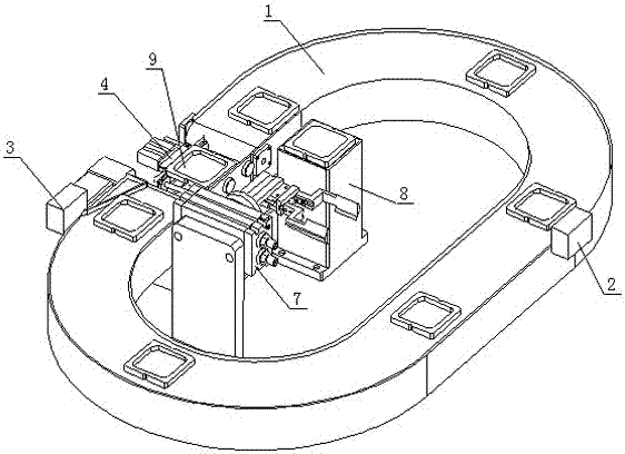
[0030] The bulk material feeding method for chip mounter of the present invention, concrete steps comprise:

[0031] Step 1. Enter or program the basic information of all types of components to be mounted and the corresponding identification code information into the control center of the placement machine.

[0032] The basic information entered includes the type, model, polarity, shape and other information of components for later recall and comparison. Among them, in order to form a one-to-one relationship, after entering the basic information, it is necessary to register and save the corresponding identification code correspondingly, so as to provide convenience for later scanning the code to confirm the type of component.

[0033] Step 2. Paste the corresponding identification codes on the side walls of the material boxes, and place the material boxes on the endless conveyor belt for automatic transmission and feeding.

[0034] The pasted identification code can be pasted...


PUM


Abstract

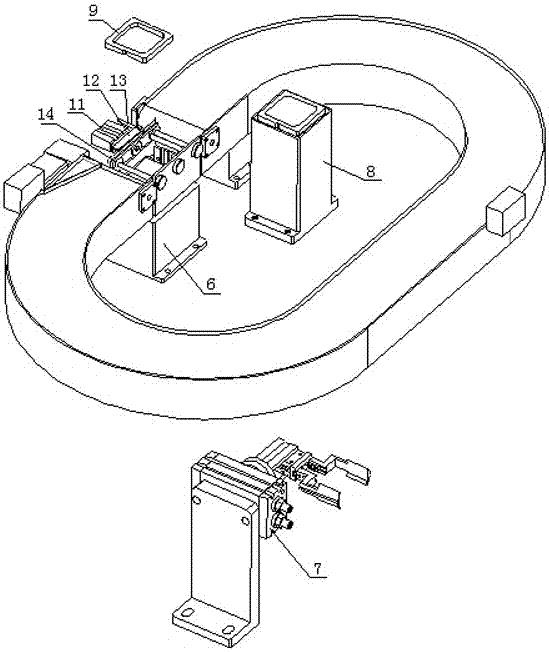
The invention discloses a bulk material feeding method and device for a chip mounter. The device comprises a cycle conveying belt, a material box, a working position, a first barcode scanner and a second barcode scanner, wherein the first barcode scanner and the second barcode scanner are arranged at one side of the cycle conveying belt, a positioning device, a transmission device and a material separation device are arranged on the working position, the material separation device is used for vibrating upwards and downwards or in a left-right direction, and the transmission device and the positioning device are connected onto the material separation mechanism. By the structure, rapid surface mounting of a bulk material in an assembly line is achieved, the re-braiding process is prevented, the surface mounting process is simplified, the surface mounting efficiency is improved, the surface mounting of various components in a few amount after verification is facilitated, and the automatic surface mounting demand of the bulk material in war industry and research units is satisfied.

Description

technical field [0001] The invention relates to an auxiliary equipment for a placement machine, in particular to a method and a device for feeding bulk materials that can be used in conjunction with a placement machine, and belongs to the field of electronic placement equipment. Background technique [0002] In the field of electronic placement technology, the placement of electronic components is a process with high technical content and complicated operations. The placement machine is a kind of main equipment to complete this kind of work. When the placement machine is working, use the computer-aided control system and the corresponding positioning system to accurately position the placement head, and automatically pick up the electronic components on the automatic feeder through the suction pen on the placement head, and then drive the placement through the transmission system The head accurately mounts the electronic components to the corresponding position of the tar...

Claims


Application Information

Patent Timeline
IPC IPC(8): H05K13/02H05K13/04H05K3/30
CPCH05K3/303H05K13/028H05K13/0417H05K13/046
Inventor 张延忠赵永先
Owner 泰姆瑞(北京)精密技术有限公司
Learn More