Positioning and transferring of substrate

A positioning platform and transmission unit technology, applied in power transmission devices, conveyors, transportation and packaging, etc., can solve the problems of long intervals of production time, time-consuming inspection and processing, occupation of printed circuit board production, etc.

Inactive Publication Date: 2017-07-21
MUTRACX INT
View PDF14 Cites 7 Cited by
  • Summary
  • Abstract
  • Description
  • Claims
  • Application Information

AI Technical Summary

Problems solved by technology

Disadvantage of the disclosed system is that although this works simultaneously, the total production time of each substrate still requires too long a time interval
Inspection and processing of batches of substrates is time consuming and takes up production of printed circuit boards

Method used


Image

  • Positioning and transferring of substrate
  • Positioning and transferring of substrate
  • Positioning and transferring of substrate

Examples


Embodiment Construction

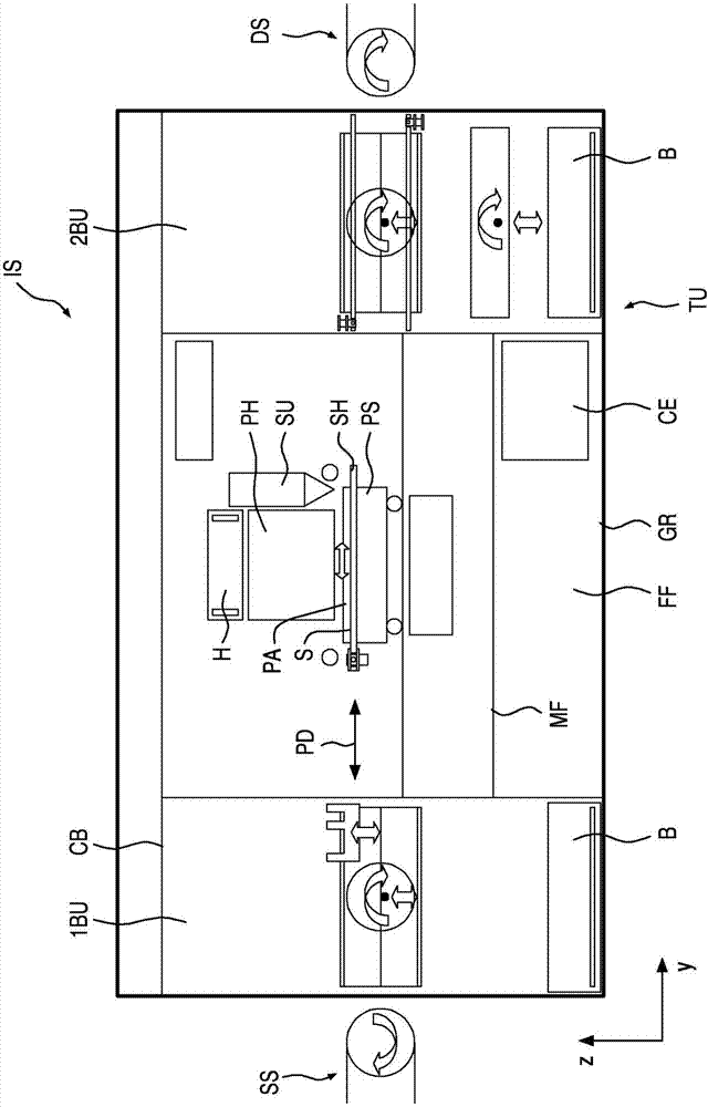
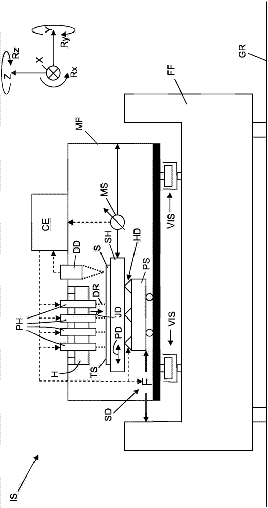
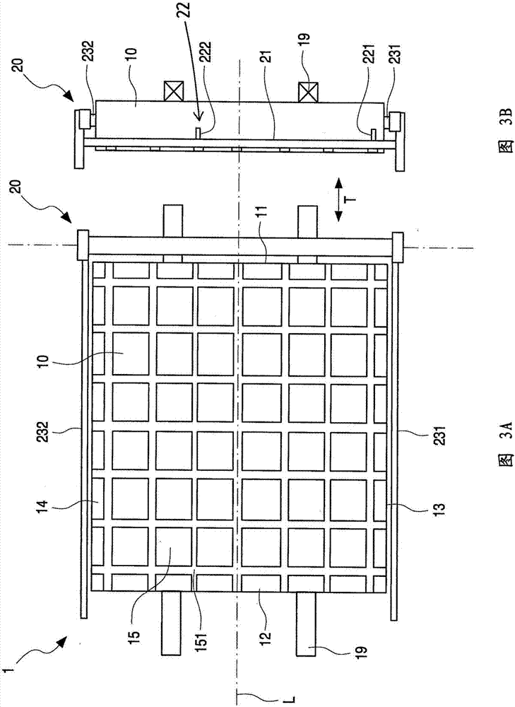
[0088] A printed circuit board, which is used to mechanically support and electrically connect electronic components, is called a PCB. A PCB is also known as a printed wiring board (PWB) or an etched wiring board. Printed circuit boards are used in nearly all of the simplest commercially manufactured electronic devices. The PCB includes a base including at least one conductive via layered etched from at least one copper sheet onto a non-conductive substrate. The base has a non-conductive substrate. The substrate typically includes resin-bonded fibers. The substrate is typically formed from a spacer insulator layered with epoxy. Boards are typically coated with a solder mask, most of which are green in color. A blank PCB, or simply called a "blank", is formed by layering a non-conductive substrate with at least one copper sheet. The blank form is used to manufacture the base product of the PCB.

[0089] Printed circuit boards can be manufactured in several ways. In order...


PUM


Abstract

The invention relates to positioning and transferring of a substrate. A substrate conveyer used for supporting a substrate in an ink jet system includes a conveyer main body, a conveyer supporting surface used for supporting the substrate and a substrate transferring unit used for conveying the substrate to the conveyer supporting surface and conveying the substrate back from the conveyor supporting surface. The substrate transferring unit includes at least one clamp used for clamping the substrate. Improvements of the substrate conveyer according to the invention are that a substrate transfer guiding device is fixed to the conveyer main body, so that in the process of movement of the substrate conveyer main body, the substrate transfer guiding device moves with the conveyer main body together. Favorably, conveying of the substrate can be executed with high precision and the substrate is then positioned on the conveyer supporting surface. Since the transfer guiding device is fixed to the conveyer main body, the substrate is more accurately placed on the conveyer supporting surface.

Description

[0001] This application is a divisional application of an invention application filed on December 28, 2012, with application number 201280071043.8 and titled "Inkjet System for Printing Printed Circuit Boards". technical field [0002] The present invention generally relates to apparatuses, methods and uses for the manufacture of substrates comprising ink patterns. In particular, the present invention relates to several aspects of methods and inkjet systems for manufacturing printed circuit boards by printing ink patterns on substrates. Background technique [0003] US2007 / 0154081 discloses a system for checking and verifying circuits. The system has a chassis that includes a first station with automated optical inspection (AOI) equipment that performs AOI of an electrical circuit to identify defects of candidate objects on the electrical circuit. Further, the chassis includes a second station having verification equipment that performs verification of defects of candidate ...

Claims


Application Information

Patent Timeline
Patent Type & Authority Applications(China)
IPC IPC(8): H05K3/06B65G54/00
CPCB41J2/01B41J2/165B41J3/407B41M5/0047B65G54/00H05K3/06B41J2/16535B41J2/16541G01N21/956H05K3/125H05K2203/1344H05K2203/013G01N2021/95638B65G2201/022G01N21/95607H05K3/0079H05K3/061G01N2021/95615H05K2203/1563H05K2203/1572H05K2203/162H01L2924/0002B41J2/16538B41J2/16544B41J2/2132B41J25/001B41J3/60H01L2924/00H05K3/22H05K1/092B05B1/08B05B12/16B05B13/0221H01L21/288H01L22/12H01L23/544H05K2203/1461H05K2203/163H05K2203/16
Inventor 亨克·扬·兹维尔斯雅各布斯·亨德里克斯·约翰内斯·扬森约斯·安妮·费尔曼
Owner MUTRACX INT
Why Eureka
Try Eureka