Minority carrier lifetime tester probe and minority carrier lifetime tester

A technology of minority carrier lifetime and tester, which is applied in the direction of single semiconductor device testing, semiconductor characterization, etc., can solve the problems of measuring semiconductor material surface unevenness, large measurement error, inconvenient use, etc., and achieve compact and reasonable structure layout and accurate voltage value , the effect of overall structural stability

Active Publication Date: 2017-07-25
SHANDONG CHENYU RARE MATERIAL TECH CO LTD
View PDF7 Cites 1 Cited by
  • Summary
  • Abstract
  • Description
  • Claims
  • Application Information

AI Technical Summary

Problems solved by technology

[0005] In order to solve the above-mentioned technical problems, the present invention provides a probe of a minority carrier lifetime tester and a minority carrier lifetime tester, which effectively solve the problem that the current probes and testers used for testing the minority carrier lifetime are bulky, inconvenient to use, and most of them are non-contact measurements and The problem of large measurement errors due to the unevenness of the surface of semiconductor materials is to provide a probe of a minority carrier lifetime tester and a minority carrier lifetime tester. The structure design is carried out by using the principle of the microwave photoconductive decay method, so that the probe can be held in any Direction movement, the host controls the laser to control the injected light source, and at the same time makes the two internal probes contact the semiconductor material, and measures the change of the voltage at both ends of the probe in real time to improve the accuracy of the measurement

Method used


Image

  • Minority carrier lifetime tester probe and minority carrier lifetime tester
  • Minority carrier lifetime tester probe and minority carrier lifetime tester
  • Minority carrier lifetime tester probe and minority carrier lifetime tester

Examples


Embodiment

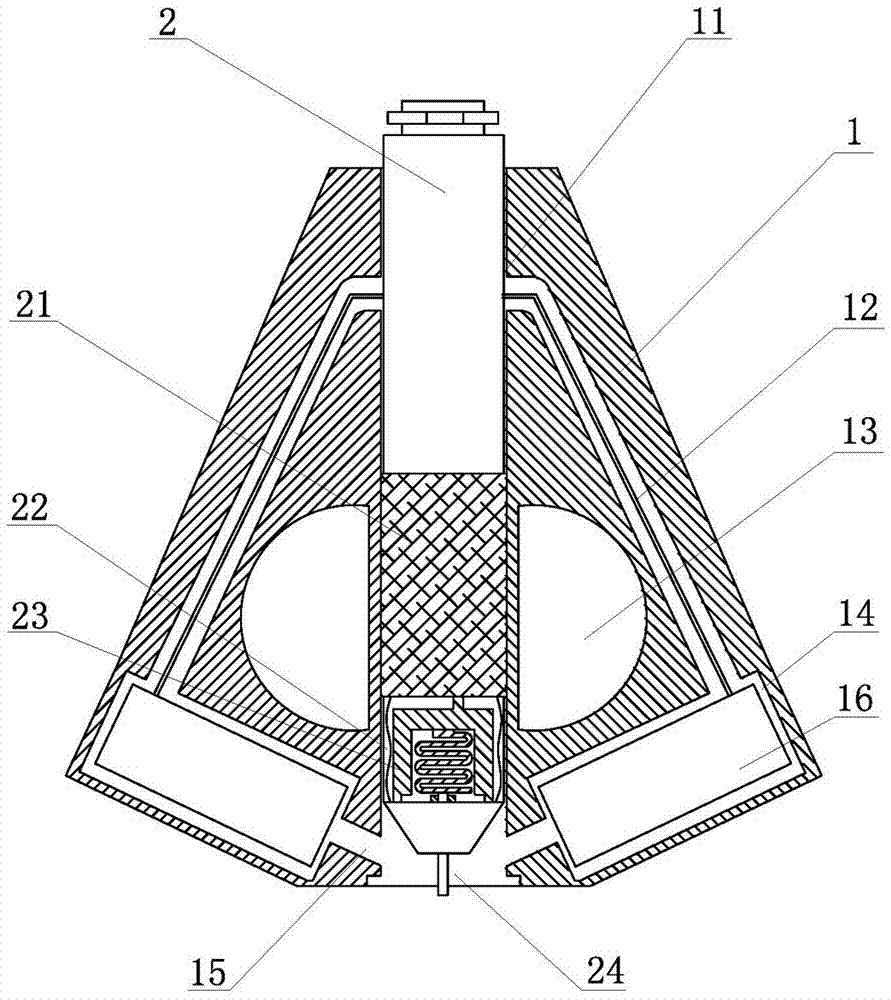
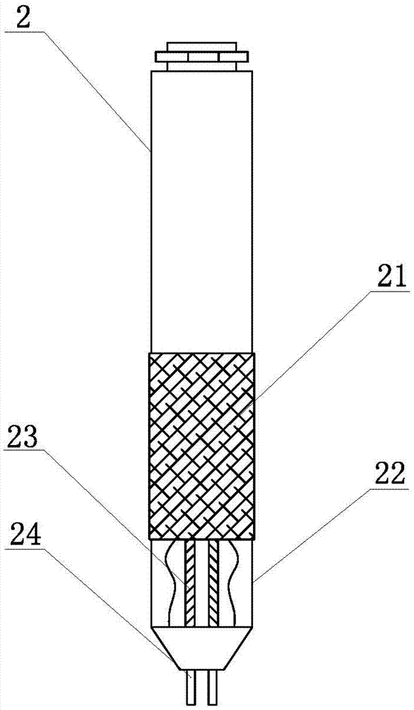
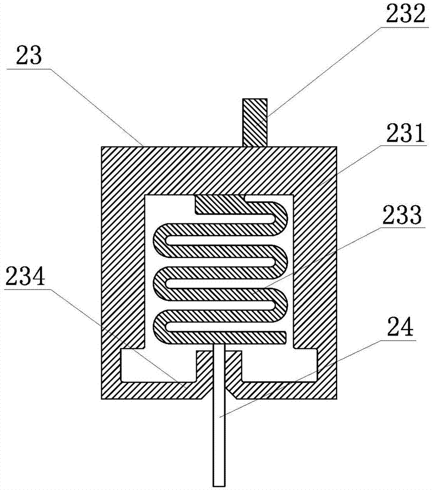
[0040] Embodiment: The process of using the present invention to measure semiconductor materials is to firstly carry out surface cleaning treatment on the semiconductor material to be measured to remove the pollutants and oil stains on the surface; Two probes 24 are in contact with the semiconductor material to be tested, and the AD acquisition module 6 in the host computer 3 monitors in real time whether the voltage value between the two probes 24 is stable through the analog input port 61, and transmits the signal to the control module 4, when the measured When the voltage value is unstable, the control module 4 prompts to re-contact until the voltage detection value is stable, and the control module 4 drives the constant current source circuit 51 in the power supply module 5 to select a suitable constant current source gear according to the resistivity of the sample. Real-time and intuitive monitoring of the unevenness of the material surface improves the accuracy of the tes...


PUM


Abstract

The invention relates to a minority carrier lifetime tester probe and a minority carrier lifetime tester and belongs to the technical field of semiconductor minority carrier lifetime testing. The probe comprises an outer housing and a probe body, and is characterized in that a cylindrical cavity is disposed in the center of the outer housing, wire pipelines are arranged on the left and right sides of the cylindrical cavity symmetrically and lead to the cylindrical cavity, laser accommodating chambers are arranged at the lower ends of the wire pipelines and communicates with the wire pipelines, laser radiation channels are arranged on the end portions of the inner side ends of the laser accommodating chambers, the probe body is provided with a wire receiving section and a probe needle clamping section from top to bottom, and fixing clamps are disposed inside the probe clamping section symmetrically in front and back and clamp a probe needle. The minority carrier lifetime tester comprises a control module and a power supply module, an AD acquisition module and a counting module which are electrically connected with the control module. The minority carrier lifetime tester probe is stable in overall structure and compact and reasonable in configuration. The minority carrier lifetime tester is more portable, more accurate in test accuracy, and suitable for popularization and application.

Description

technical field [0001] The invention relates to the technical field of semiconductor minority carrier lifetime testing, in particular to a minority carrier lifetime tester probe and a minority carrier lifetime tester. Background technique [0002] Minority carrier lifetime (referred to as minority carrier lifetime) is an important parameter of semiconductor materials, which has an important impact on the performance of semiconductor devices and the efficiency of solar cells. The minority carrier lifetime of semiconductor materials is one of the important parameters for evaluating semiconductor materials. As the basis for process adjustment and material differentiation, accurate measurement of minority carrier lifetime has important practical significance. [0003] The microwave photoconductive decay method is used to test the minority carrier lifetime, including two processes of electron-hole pairs generated by light injection and changes of microwave detection signals. La...

Claims


Application Information

Patent Timeline
Patent Type & Authority Applications(China)
IPC IPC(8): G01R31/26
CPCG01R31/2648
Inventor 李杰于友刘世伟石坚
Owner SHANDONG CHENYU RARE MATERIAL TECH CO LTD
Why Eureka
Try Eureka