
Display panel and electronic equipment
A display panel and area technology, applied in the direction of circuits, electrical components, electric solid devices, etc., can solve the problems affecting the fingerprint recognition accuracy of fingerprint recognition modules, achieve the effects of reducing noise, reducing stray light and improving accuracy
- Summary
- Abstract
- Description
- Claims
- Application Information
AI Technical Summary
Problems solved by technology
Method used
Image

Examples
Embodiment Construction
[0064] The present invention will be further described in detail below in conjunction with the accompanying drawings and embodiments. It should be understood that the specific embodiments described here are only used to explain the present invention, rather than to limit the present invention. In addition, it should be noted that, for the convenience of description, only some parts related to the present invention are shown in the drawings but not all structures.
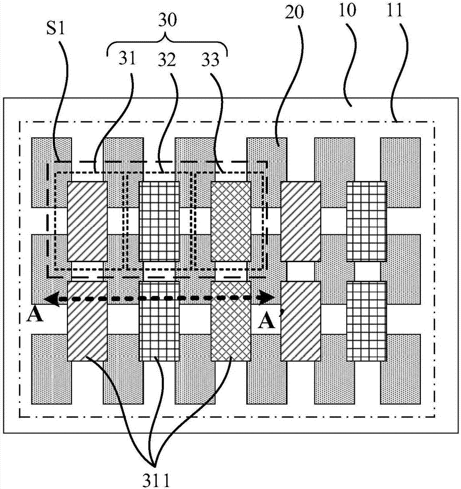
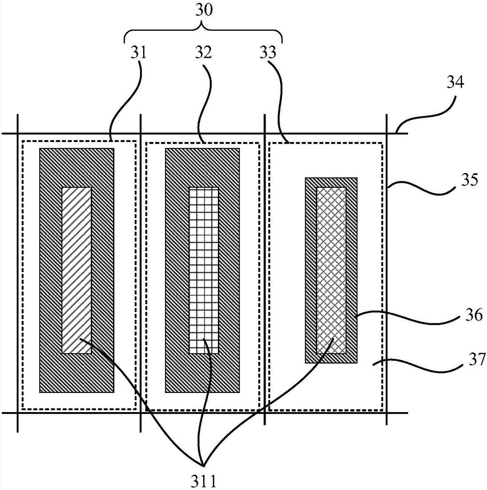
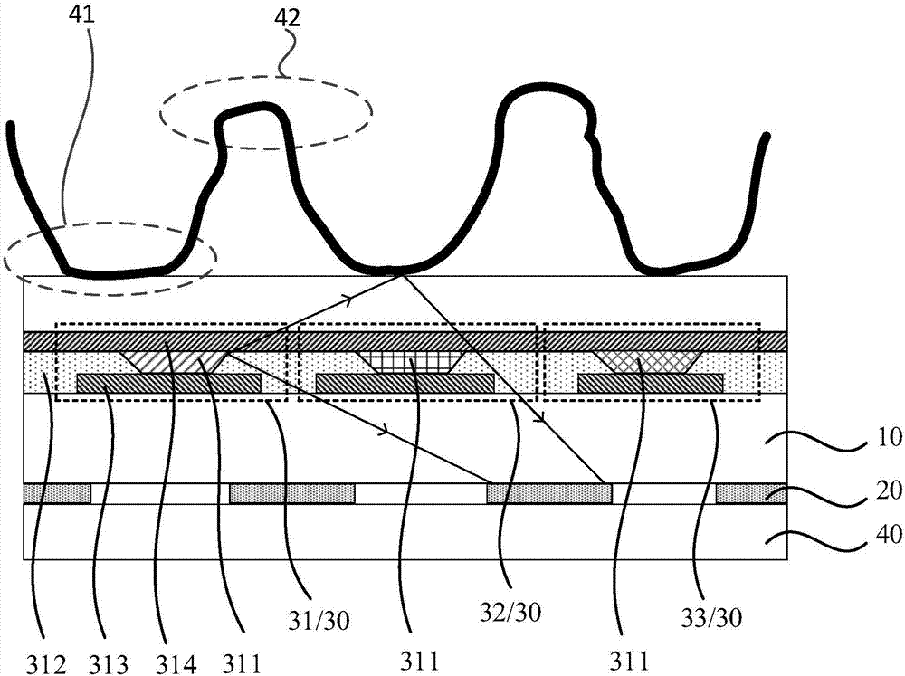
[0065] Figure 1a It is a schematic top view structural diagram of a display panel provided by an embodiment of the present invention, Figure 1b It is a partially enlarged schematic diagram of the S1 area in Fig. 1a, Figure 1c for along Figure 1a Schematic diagram of the cross-sectional structure in the direction of AA', refer to Figure 1a , Figure 1b with Figure 1c , the display panel provided by the embodiment of the present invention includes an array substrate 10 , a plurality of organic light emitting ...
PUM
 Abstract
Description
Claims
Application Information