OLED array substrate, manufacturing method and display apparatus thereof

A technology of array substrates and substrate substrates, which is applied in semiconductor/solid-state device manufacturing, electrical components, electric solid-state devices, etc., and can solve problems such as large cathode impedance, poor film quality, and abnormal OLED display

Active Publication Date: 2017-07-28
BOE TECH GRP CO LTD
View PDF4 Cites 30 Cited by
  • Summary
  • Abstract
  • Description
  • Claims
  • Application Information

AI Technical Summary

Problems solved by technology

[0003] However, there are still some serious problems in OLED display technology at present, which limit the development of OLED display technology.
For example, when the OLED display device has a common cathode, the cathode of the OLED display device is usually formed by evaporation or sputtering. Due to the...

Method used


Image

  • OLED array substrate, manufacturing method and display apparatus thereof
  • OLED array substrate, manufacturing method and display apparatus thereof
  • OLED array substrate, manufacturing method and display apparatus thereof

Examples


Embodiment Construction

[0034] The following will clearly and completely describe the technical solutions in the embodiments of the present invention with reference to the accompanying drawings in the embodiments of the present invention. Obviously, the described embodiments are only some, not all, embodiments of the present invention. Based on the embodiments of the present invention, all other embodiments obtained by persons of ordinary skill in the art without making creative efforts belong to the protection scope of the present invention.

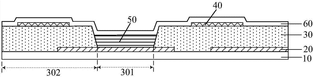
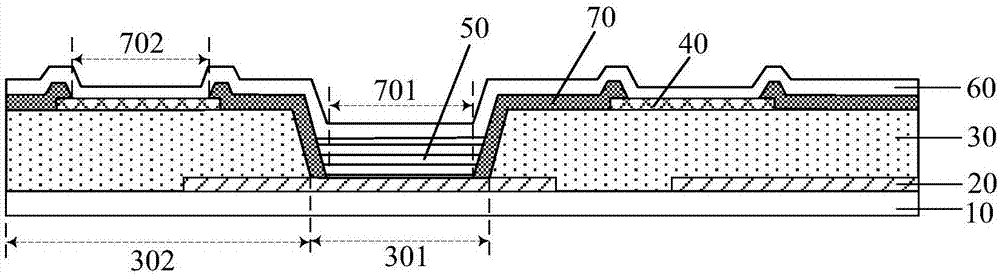
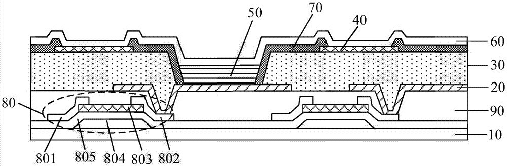
[0035] An embodiment of the present invention provides an OLED array substrate, such as Figure 1-Figure 4 shown, including:

[0036] The first electrode layer arranged on the base substrate 10, the first electrode layer includes a plurality of first electrodes 20; the first pixel defining layer 30, the first pixel defining layer 30 is arranged on the first electrode layer, the first pixel defining The layer 30 includes an opening area 301 and a pixel definin...


PUM


Abstract

An embodiment of the invention provides an OLED array substrate, a manufacturing method and a display apparatus thereof and relates to the display technology field. A resistance of a second electrode layer can be reduced. The OLED array substrate comprises a first electrode layer, a first pixel definition layer, an auxiliary electrode, an organic layer and the second electrode layer, wherein the first electrode layer is arranged on a substrate and includes a plurality of first electrodes; the first pixel definition layer is arranged on the first electrode layer and includes opening areas and a pixel definition area used for defining the opening areas, and one first electrode is exposed from each opening area; the auxiliary electrode is arranged on the first pixel definition layer and is located in the pixel definition area; the organic layer is arranged in the opening areas of the first pixel definition layer; and the second electrode layer is arranged on the organic layer and the auxiliary electrode, and the second electrode is contacted with the auxiliary electrode and the organic layer. The method and the display apparatus are used for the OLED array substrate.

Description

technical field [0001] The invention relates to the field of display technology, in particular to an OLED array substrate, a preparation method thereof, and a display device. Background technique [0002] OLED (Organic Light Emitting Diode, Organic Light Emitting Diode) display technology has received great attention and development for a long time due to its many advantages such as self-illumination, fast response, high brightness, and thinness. Currently, the OLED display technology has been mass-produced in mobile products and TV (Television, television) products. [0003] However, there are still some serious problems in OLED display technology at present, which limit the development of OLED display technology. For example, when the OLED display device has a common cathode, the cathode of the OLED display device is usually formed by evaporation or sputtering. Due to the low temperature of the evaporation or sputtering process, the film quality is poor, so the impedance ...

Claims


Application Information

Patent Timeline
IPC IPC(8): H01L27/32H01L51/52H01L51/56
CPCH10K59/122H10K59/1315H10K50/814H10K50/824H10K71/00
Inventor 舒适徐传祥
Owner BOE TECH GRP CO LTD
Why Eureka
Try Eureka