Light-emitting diode chip having temperature compensation of the wavelength

一种芯片、温度变化的技术,应用在电气元件、电路、半导体器件等方向,能够解决温度影响改变色彩印象、亮度减小、敏感度降低等问题

Active Publication Date: 2017-08-01
OSRAM OPTO SEMICON GMBH & CO OHG
View PDF5 Cites 1 Cited by
  • Summary
  • Abstract
  • Description
  • Claims
  • Application Information

AI Technical Summary

Problems solved by technology

[0005] It is also known that the human eye is less sensitive at wavelengths above about 560nm
In optoelectronic semiconductor chips that emit at higher wavelengths, for this reason a temperature-dependent increase in the emission wavelength can lead not only to a changed color impression, but also to a visually perceived reduction in brightness

Method used


Image

  • Light-emitting diode chip having temperature compensation of the wavelength
  • Light-emitting diode chip having temperature compensation of the wavelength
  • Light-emitting diode chip having temperature compensation of the wavelength

Examples


Embodiment Construction

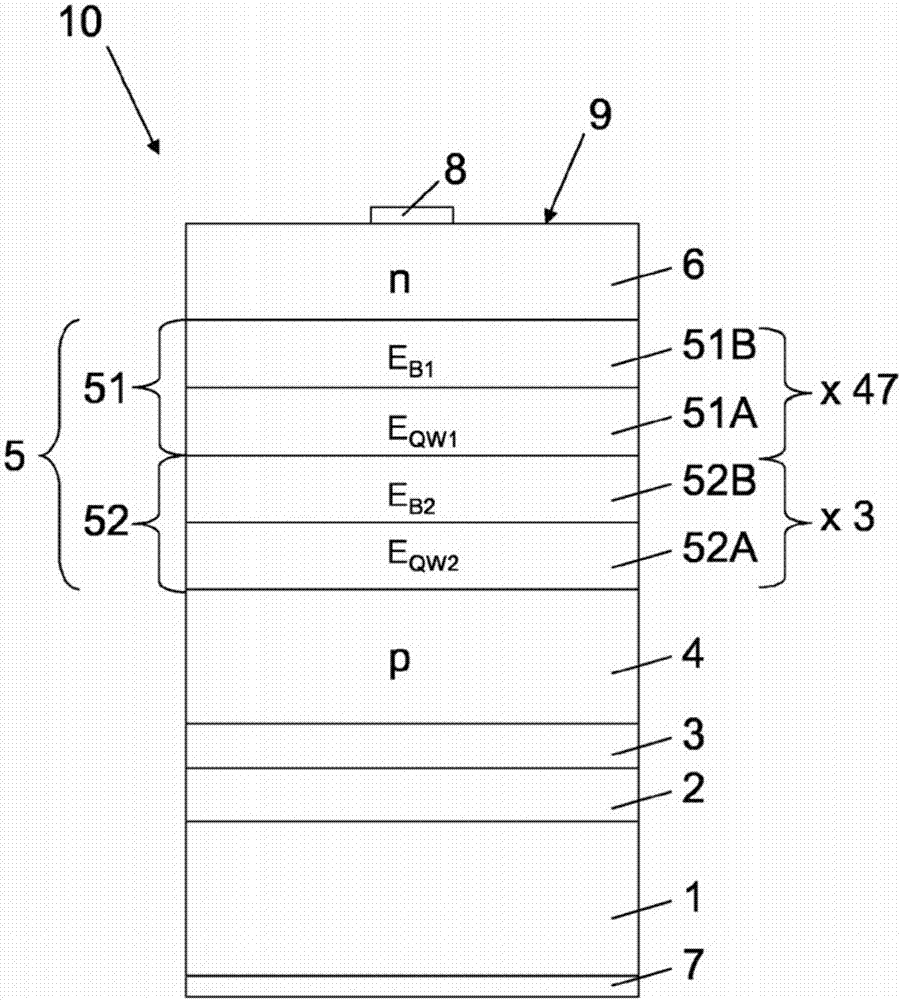
[0028] exist figure 1The optoelectronic semiconductor chip 10 according to one embodiment shown in is an LED chip with a p-type semiconductor region 4, an n-type semiconductor region 6 and a An active layer 5 suitable for emitting radiation. This embodiment of the optoelectronic semiconductor chip is a so-called thin-film semiconductor chip from which the growth substrate initially used for the epitaxial growth of the semiconductor layers 4 , 5 , 6 is peeled off and the semiconductor layer sequence is instead deposited by means of The connection layer 2 , in particular the solder layer, is connected to a carrier substrate 1 different from the growth substrate.

[0029] In such a thin-film light-emitting diode chip 10 , the p-type semiconductor region 4 generally faces the carrier substrate 1 . A mirror layer 3 is advantageously arranged between the p-type semiconductor region 4 and the carrier substrate 1 , which advantageously deflects radiation emitted in the direction of...


PUM


Abstract

The invention relates to an optoelectronic semiconductor chip (10), comprising: a p-type semiconductor region (4), an n-type semiconductor region (6), an active layer (5), which is arranged between the p-type semiconductor region (4) and the n-type semiconductor region (6) and which is designed as a multiple quantum well structure (51, 52), wherein the multiple quantum well structure (51, 52) has a first region (51) of alternating first quantum well layers (51A) and first barrier layers (51B) and a second region having at least one second quantum well layer (52A) and at least one second barrier layer (52B), the at least one second quantum well layer (52A) has an electronic band gap (E QW2) that is less than the electronic band gap (E QW1) of the first quantum well layers (51A), the at least one second barrier layer (52B) has an electronic band gap (E B2) that is greater than the electronic band gap (E B1) of the first barrier layers (51B).

Description

technical field [0001] The invention relates to an optoelectronic semiconductor chip. [0002] Cross-References to Related Applications [0003] This application claims priority from German patent application 10 2014 117 611.1, the disclosure content of which is hereby incorporated by reference. Background technique [0004] The optical and electronic properties of semiconductor materials are primarily determined by the bandgap, the energy gap between the valence and conduction bands. The bandgap of semiconductor materials generally decreases with increasing temperature. In radiation-emitting optoelectronic semiconductor chips, such as LEDs or semiconductor lasers, this can result in an increase in the wavelength of the emitted radiation with increasing operating temperature. The color impression of the emitted radiation can thereby be changed. [0005] It is also known that the sensitivity of the naked eye decreases at wavelengths above about 560 nm. In optoelectronic ...

Claims


Application Information

Patent Timeline
Patent Type & Authority Applications(China)
IPC IPC(8): H01L33/06H01L33/08
CPCH01L33/06H01L33/08
Inventor 安德烈亚斯·鲁道夫彼得鲁斯·松德格伦伊瓦尔·通林
Owner OSRAM OPTO SEMICON GMBH & CO OHG
Why Eureka
Try Eureka