Display panel and manufacturing method thereof, and display device

A display panel and display surface technology, applied in the fields of display panels and display devices, can solve the problems of increasing space, reducing production efficiency, and low utilization rate of substrate substrates, so as to increase contact area, improve yield, and prevent punching. and the effect of the risk of conductive material fill failure

Active Publication Date: 2017-08-11
BOE TECH GRP CO LTD +1
View PDF6 Cites 40 Cited by
  • Summary
  • Abstract
  • Description
  • Claims
  • Application Information

AI Technical Summary

Problems solved by technology

In this way, although the display failure phenomenon caused by cracks in the inorganic insulating layer is avoided to a certain extent, two Mask processes are added, which increases the difficulty of the process and the manufacturing cost, and reduces the production efficiency.
In addition, the formation of the c

Method used


Image

  • Display panel and manufacturing method thereof, and display device
  • Display panel and manufacturing method thereof, and display device
  • Display panel and manufacturing method thereof, and display device

Examples


Embodiment Construction

[0048] The specific implementation manners of the display panel provided by the embodiments of the present invention, its manufacturing method and the display device will be described in detail below with reference to the accompanying drawings.

[0049] The thickness, shape and size of each film layer in the drawings do not reflect the true proportion of the display panel, but are only intended to schematically illustrate the content of the present invention.

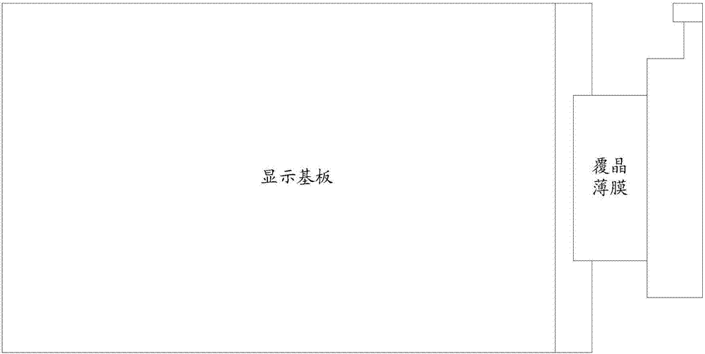
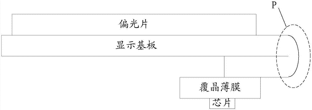
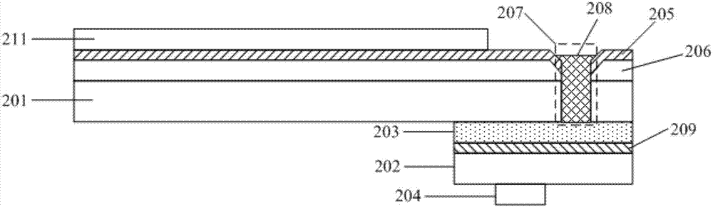
[0050] A display panel provided by an embodiment of the present invention, such as Figure 2a As shown, it includes: a display substrate 201, a chip-on-film 202 arranged on the side away from the display surface of the display substrate 201, an adhesive 203 arranged between the display substrate 201 and the chip-on-film 202, and a chip fixed on the chip-on-film 202 away from the integrated circuit chip 204 on the side of the display substrate 201; wherein,

[0051] The COF 202 is fixed on the side of the display substr...


PUM

PropertyMeasurementUnit
Apertureaaaaaaaaaa
Diameteraaaaaaaaaa

Abstract

The invention discloses a display panel and a manufacturing method thereof, and a display device. After a chip on film is adhered by adhesive to a side away from the display surface of a display substrate, signal lines around the display surface of the display substrate can be connected with connecting terminals arranged on the chip on film through a conductive material arranged in connecting holes which at least penetrate through the display substrate, the signal lines and an insulating layer. Thus, a connecting terminal bending process is omitted, there is no connecting terminal bending area around a display panel, and the display panel has a narrower bezel. Moreover, as the insulating layer is provided with multiple depressions around the connecting holes, the conductive material can be in contact with the surfaces of the signal lines in the depressions, the contact area of the conductive material and the signal lines is increased, hole drilling and conductive material filling failure are prevented, and the yield of the product is improved.

Description

technical field [0001] The invention relates to the field of display technology, in particular to a display panel, a manufacturing method and a display device. Background technique [0002] With the continuous advancement of display technology, display panels are more and more widely used in display products. Display products with narrow bezels (Narrow Bezel) have attracted a large number of consumers because they can enable users to obtain a better viewing experience. [0003] Currently, bending the connection terminals is the only solution to realize display products with narrow bezels. However, there are many problems with the yield rate of the display products manufactured by the connecting terminal bending process. For example, in the Figure 1a The shown display products when bent, such as Figure 1b The inorganic insulating layer in the bending region P of the connecting terminal shown is prone to cracks, which will lead to display failure. In the prior art, a mask...

Claims


Application Information

Patent Timeline
IPC IPC(8): H01L23/485H01L23/488H01L21/60H01L25/18
CPCH01L24/32H01L24/83H01L25/18H01L2224/0231H01L2224/0233H01L2224/02381H01L2224/32146H01L2224/83G06F1/1656G06F1/1626G06F1/1658H01L27/124G06F1/189
Inventor 王本莲董向丹黄炜赟高永益
Owner BOE TECH GRP CO LTD
Why Eureka
Try Eureka