Display substrate and display device

A display substrate and display area technology, which is applied in semiconductor devices, electrical components, circuits, etc., can solve the problems of increasing power consumption of display devices, inability to achieve narrow borders, and increasing IRdrop

Inactive Publication Date: 2017-08-18
BOE TECH GRP CO LTD +1
View PDF2 Cites 25 Cited by
  • Summary
  • Abstract
  • Description
  • Claims
  • Application Information

AI Technical Summary

Problems solved by technology

If the width of the signal line 14 is small, it is beneficial to realize the narrow frame, but it will cause the contact area between the first electrode layer 11 and the signal line 14 to be small, and the contact resistance will increase, thereby increasing the IR drop (resistance voltage drop) , increase the power consumption of the display device; if the IR drop is to be reduced, the contact area between the first electrode layer 11 and the signal line 14 must be increased, and since the length of the signal line 14 is constant, the increase in the contact area is It is necessary to increase the width of the signal line 14, so that narrow borders cannot be realized

Method used


Image

  • Display substrate and display device
  • Display substrate and display device
  • Display substrate and display device

Examples


Embodiment Construction

[0026] Specific embodiments of the present invention will be described in detail below in conjunction with the accompanying drawings. It should be understood that the specific embodiments described here are only used to illustrate and explain the present invention, and are not intended to limit the present invention.

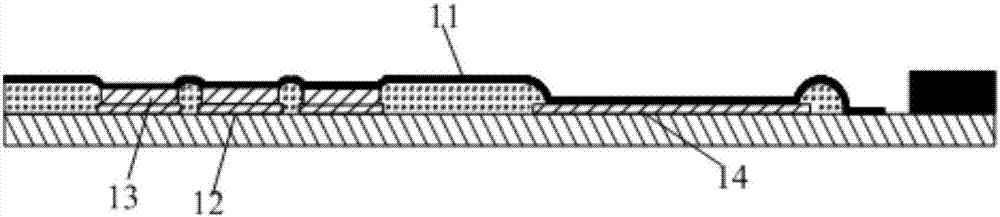
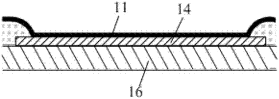
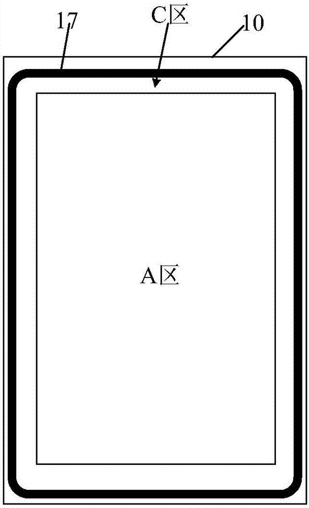
[0027] As an aspect of the present invention, a display substrate is provided, image 3 It is a schematic diagram of the division of each area on the array substrate provided by the present invention; Figure 4 is a partial structural schematic diagram of the array substrate; Figure 5 Yes Figure 4 The schematic diagram of the contact part between the first electrode layer and the signal line. combine Figure 3 to Figure 5 As shown, the display substrate includes a substrate 10, the substrate 10 includes a display area (A area) and a non-display area (B area) surrounding the display area, the non-display area (B area) is provided with signal lines 14, and t...


PUM


Abstract

The present invention provides a display substrate, which includes a substrate. The substrate comprises a display area and a non-display area configured to surround the display area. The non-display area is provided with a signal line. The display area is provided with a plurality of light-emitting units. A first electrode layer is also arranged above the substrate. The first electrode layer comprises an electrode part and a transmission part. The electrode part is located in the display area and is arranged above the plurality of light-emitting units. The transmission part is located in the non-display area and is arranged on the upper surface of the signal line. The area of the contact part of the signal line with the transmission part is larger than the orthographic projection area of the above contact part on the substrate. Correspondingly, the invention further provides a display device. According to the technical scheme of the invention, the narrow-frame design can be realized, and the IR drop can be reduced.

Description

technical field [0001] The present invention relates to the field of display technology, in particular to a display substrate and a display device. Background technique [0002] Organic Light Emitting Diode (OLED) devices are widely used because of their advantages such as self-illumination, rich colors, fast response, wide viewing angle, light weight, thin thickness, low power consumption, and flexible display. It is worth noting that organic electroluminescent display devices made of organic electroluminescent devices also have great application prospects. [0003] figure 1 It is a structural schematic diagram of a display substrate in an existing organic electroluminescent display device, figure 2 Yes figure 1 The schematic diagram of the contact part between the first electrode layer and the signal line, combined with figure 1 and figure 2 As shown, a plurality of light-emitting units 13 are arranged above the substrate, and a plurality of light-emitting units 13 ...

Claims


Application Information

Patent Timeline
IPC IPC(8): H01L27/32
CPCH10K59/1315H10K59/131
Inventor 吴建鹏罗昶
Owner BOE TECH GRP CO LTD
Why Eureka
Try Eureka