DDR SDRAM control circuit, DDR SDRAM chip, PCB and electronic equipment

A technology for controlling circuits and clock circuits, applied in the fields of DDRSDRAM control circuits, DDRSDRAM chips, PCB boards and electronic equipment, can solve the problems of multiple clock connections, low clock frequency, unbalanced delay, etc.

Active Publication Date: 2017-08-25
APPOTECH
View PDF4 Cites 10 Cited by
  • Summary
  • Abstract
  • Description
  • Claims
  • Application Information

AI Technical Summary

Problems solved by technology

[0004] An object of the embodiments of the present invention is to provide a DDR SDRAM control circuit, DDR SDRAM chip, PCB board and electronic equipment, which solves the low clock frequency and more clock connections of the read and write operations of the existing DDR SDRAM controller And complex, resulting in unbalanced technical problems

Method used


Image

  • DDR SDRAM control circuit, DDR SDRAM chip, PCB and electronic equipment
  • DDR SDRAM control circuit, DDR SDRAM chip, PCB and electronic equipment
  • DDR SDRAM control circuit, DDR SDRAM chip, PCB and electronic equipment

Examples


Embodiment Construction

[0034] In order to make the object, technical solution and advantages of the present invention clearer, the present invention will be further described in detail below in conjunction with the accompanying drawings and embodiments. It should be understood that the specific embodiments described here are only used to explain the present invention, not to limit the present invention.

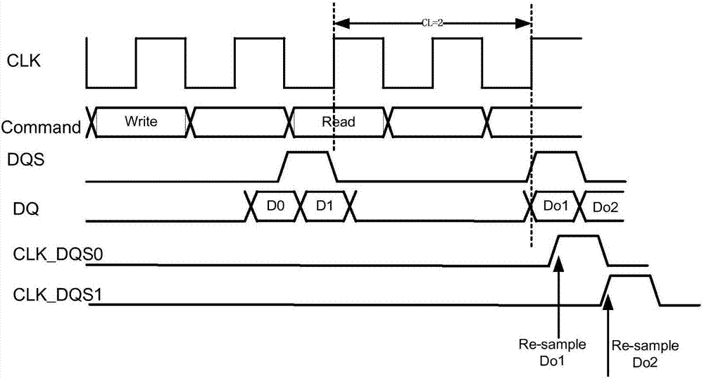
[0035] For a DDR SDRAM memory connected to the chip, it needs to accurately determine the position of the clock signal and the data strobe pulse DQS in the address, control and data signals. Such as figure 1As shown, in a DDR SDRAM clock cycle, there are two data pulses DQ (data signal) per cycle, and one data pulse per half cycle. When the data pulse DQ is stable within a half cycle (for example, in the middle of a half cycle), it is usually necessary to issue a data strobe pulse DQS. Gating a data pulse DQ at a stable point is required to correctly read or write data to the DDR SDRAM memory.

...


PUM


Abstract

The invention relates to the technical field of integrated circuits, in particular to a DDR SDRAM control circuit, a DDR SDRAM chip, a PCB and electronic equipment. The DDR SDRAM control circuit comprises a delayed phase-locked loop, a clock circuit, a clock phase selector and a logic controller, wherein the delayed phase-locked loop is used for generating a preset clock signal; the clock circuit is used for generating a reference clock signal, the frequency of which is at least doubled; and the logic controller d for controlling a data strobe pulse DQS to be centrally aligned with a data pulse DQ according to the reference clock signal when a writing operation is carried out. Compared with the clock signal of the existing DDR SDRAM control circuit, the reference clock signal is a clock signal, the frequency of which is at least doubled, so that the low-frequency clock signals are replaced by high-frequency clock signals, the designers can decrease or shorten the length of high-speed clock wires connected to interface modules, and then benefit is brought to the balance the delayed control.

Description

technical field [0001] The invention relates to the technical field of integrated circuits, in particular to a DDR SDRAM control circuit, a DDR SDRAM chip, a PCB board and electronic equipment. Background technique [0002] In the application of SOC chip (System-on-a-Chip), for the double data rate synchronous dynamic random access memory (Double Data Rate SDRAM, DDR SDRAM) controller design, since the frequency of transmission data is as high as 400MHz, the clock frequency is 200MHz, In the read operation, and the data strobe (DQ Strobe, DQS) and the data pulse DQ (Data) are edge-aligned (Edge-Aligned), the DDR SDRAM controller needs to sample data and latch data in a short time to achieve 2 data samples are sampled in one clock cycle. However, during the write operation, due to the need for DQS and DQ center-aligned (Center-Aligned), the DDR SDRAM controller needs to combine clock edges with a difference of 1 / 4 clock cycle, and the existing technology adopts a relatively ...

Claims


Application Information

Patent Timeline
Patent Type & Authority Applications(China)
IPC IPC(8): G11C11/4076G11C7/10
CPCG11C7/1066G11C7/1093G11C11/4076
Inventor 莫昌文
Owner APPOTECH
Why Eureka
Try Eureka