

Measurement device and measurement method for stray inductance in IGBT module
A stray inductance, internal module technology, applied in measuring devices, measuring electrical variables, measuring resistance/reactance/impedance, etc., can solve the problems affecting the safe working margin and error of IGBT chips, and achieve compact structure, easy to build, Overall design ingenious effect
Pending Publication Date: 2017-08-29
CHINA UNIV OF MINING & TECH
View PDF5 Cites 20 Cited by
- Summary
- Abstract
- Description
- Claims
- Application Information
AI Technical Summary
Problems solved by technology
The IGBT module is composed of two parts, the IGBT chip and the package. There is a certain parasitic inductance in the package, which affects the safe working margin of the IGBT chip.
At present, there are relatively few studies on the extraction of parasitic inductance of the IGBT internal package. The conventional method is to use finite element analysis and simulation. However, this method can only estimate the parasitic inductance parameters of the IGBT when it leaves the factory. error
Method used
View moreImage
Smart ImageViewing Examples

Examples
Embodiment 1
Embodiment 2
Login to View More PUM
 Abstract
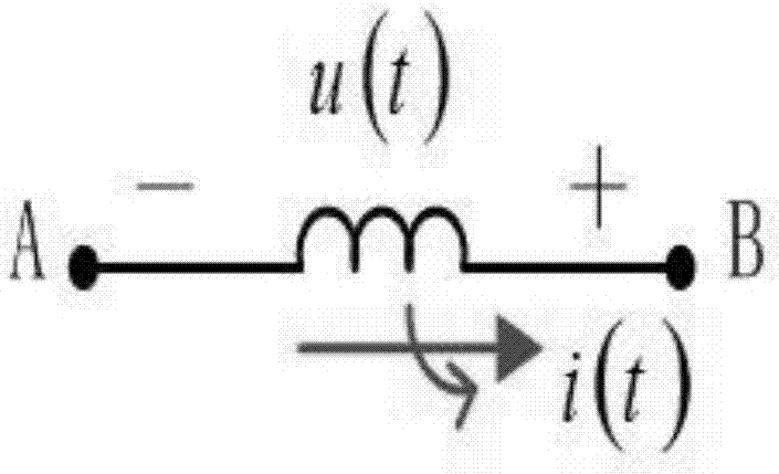
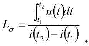
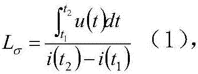
The invention relates to a measurement device for stray inductance in an IGBT module. The measurement device is characterized in that the measurement device comprises a power supply device, a to-be-measured IGBT module, a current probe, a voltage probe, an oscilloscope, a pulse triggering device, controllable switches S1, S2, S3, a DC capacitor C1, a DC discharging resistor R1, a load inductor L1 and a freewheeling diode D1; the controllable switch S2 is serially connected with the DC discharging resistor R1 and is parallelly connected with the DC capacitor C1; the freewheeling diode D1, the controllable switch S3 and the to-be-measured IGBT module are serially connected; the pulse triggering device is connected with the controllable switch S3; and the load inductor L1 is parallelly connected with two sides of the freewheeling diode D1. The measurement device can effectively evaluate induction voltage of an inner packaging parasitic parameter when the IGBT module is in a switching-off transient state. The packaged stray inductance which is calculated according to the voltage and current over two ends of a parasitic inductor is more practical and can be used for evaluating an IGBT safety margin, and furthermore can be used for verifying IGBT module designing. The measurement device and the measurement method have a certain meaning to semiconductor manufacturers and IGBT application parties.
Description
IGBT module internal stray inductance measurement device and measurement method technical field The invention relates to a measuring device, in particular to a device for measuring stray inductance inside an IGBT module, and belongs to the technical field of power electronics. Background technique IGBT modules are widely used in the power electronics industry. The IGBT module is composed of two parts, the IGBT chip and the package. There is a certain parasitic inductance in the package, which affects the safe working margin of the IGBT chip. At present, there are relatively few studies on the extraction of parasitic inductance of the IGBT internal package. The conventional method is to use finite element analysis and simulation. However, this method can only estimate the parasitic inductance parameters of the IGBT when it leaves the factory. error. Contents of the invention The present invention aims at the technical problems existing in the prior art, and provides a ...
Claims
Login to View More Application Information
Patent Timeline
 IPC IPC(8): G01R27/26
CPCG01R27/26
Inventor 何凤有耿程飞封安波谭国俊张经纬范长海
Owner CHINA UNIV OF MINING & TECH