Unlock instant, AI-driven research and patent intelligence for your innovation.

non-volatile memory device

A non-volatile storage and device technology, applied in the direction of information storage, static memory, memory system, etc., can solve problems such as the limitation of two-dimensional flash memory to improve integration

Active Publication Date: 2021-10-22
SAMSUNG ELECTRONICS CO LTD
View PDF6 Cites 0 Cited by
  • Summary
  • Abstract
  • Description
  • Claims
  • Application Information

AI Technical Summary

Problems solved by technology

However, considering the manufacturing process, conventional 2D flash memory has limitations in increasing integration

Method used


Image

  • non-volatile memory device
  • non-volatile memory device
  • non-volatile memory device

Examples


Embodiment Construction

[0023] Example embodiments will now be described more fully with reference to the accompanying drawings, in which some example embodiments are shown.

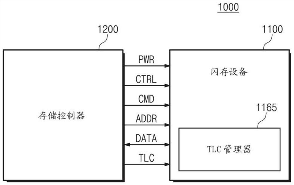
[0024] figure 1 is a block diagram of a flash memory system 1000 according to an example embodiment of the present disclosure. refer to figure 1 , the flash memory system 1000 may include a flash memory device 1100 and a storage controller 1200 . Flash memory system 1000 may include any flash memory-based data storage media, such as memory cards, universal serial bus (USB) memory, and solid state drives (SSD).

[0025] The flash memory device 1100 may perform erase, write, and read operations under the control of the memory controller 1200 . For this, the flash memory device 1100 may receive a command CMD, an address ADDR, data DATA, and a target latch command TLC via an input / output line. The target latch command TLC may be a target latch address.

[0026] The flash memory device 1100 may receive power PWR via a power lin...


PUM


Abstract

A nonvolatile memory device comprising a nonvolatile memory cell array, a page buffer circuit, a data input / output circuit, and control logic, wherein N bits are stored in a single memory cell (N is an integer greater than or equal to 2 ), the page buffer circuit is electrically connected to the nonvolatile memory cell array. The page buffer circuit includes at least N latches configured to temporarily store data. A data input / output circuit connected to the page buffer circuit receives programmed input data and provides the input data to the page buffer circuit. The control logic controls the page buffer circuit and initializes the value of the target latch before receiving all input data for programming cells from the data input / output circuit.

Description

[0001] Cross References to Related Applications [0002] This patent application claims priority from Korean Patent Application No. 10-2016-0021109 filed on February 23, 2016, the entire contents of which are incorporated herein by reference. technical field [0003] The present disclosure relates to semiconductor memory devices, and more particularly, to nonvolatile memory devices. Background technique [0004] A semiconductor memory device may include volatile memory such as DRAM and / or SRAM. The semiconductor storage device may also include nonvolatile memory such as EEPROM, FRAM, PRAM, MRAM, flash memory, and the like. Volatile memory can lose data stored in it when power is lost, while non-volatile memory retains data stored in it even when power is lost. Specifically, flash memory devices may have advantages such as high programming speed, low power consumption, large storage capacity, and the like. For this reason, flash memory systems including flash memory device...

Claims


Application Information

Patent Timeline
Patent Type & Authority Patents(China)
IPC IPC(8): G06F3/06
CPCG06F3/0607G06F3/0656G06F3/0658G06F3/0679G11C7/106G11C7/1087G11C11/5628G11C16/08G06F12/0246G06F3/061G06F3/0655G06F3/0688G11C11/5635G11C11/5642G11C16/3459
Inventor 郑凤吉金炯坤
Owner SAMSUNG ELECTRONICS CO LTD