Circuit substrate and method of manufacturing same

A technology for circuit boards and circuit parts, applied in the directions of printed circuit manufacturing, printed circuits, printed circuits, etc., can solve the problems of increasing the overall thickness of components and reducing the installation area, and achieve the effect of increasing strength

Inactive Publication Date: 2017-08-29
TAIYO YUDEN KK
View PDF7 Cites 6 Cited by
  • Summary
  • Abstract
  • Description
  • Claims
  • Application Information

AI Technical Summary

Problems solved by technology

Among them, in the case of using a flexible circuit board or the like for connection between the main circuit board and the module, although a method of using a connector and a method of bonding the component circuit board and the flexible circuit board are known, the reduction of the mounting area, the The increase in the overall thickness of the module becomes a problem

Method used


Image

  • Circuit substrate and method of manufacturing same
  • Circuit substrate and method of manufacturing same
  • Circuit substrate and method of manufacturing same

Examples


no. 1 approach >

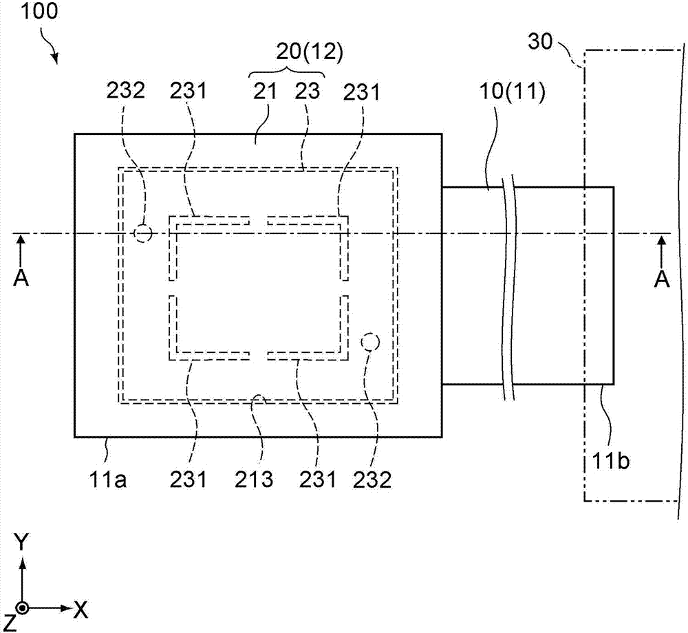
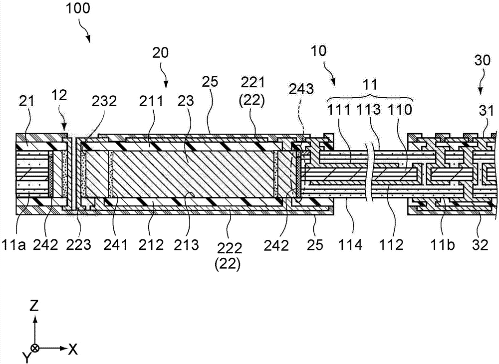
[0040] figure 1 It is a schematic plan view showing the structure of a circuit board according to an embodiment of the present invention. figure 2 Yes figure 1 A-A line direction sectional view of . Wherein, the X-axis, Y-axis and Z-axis in each figure represent the three-axis directions orthogonal to each other, and the Z-axis direction corresponds to the thickness direction of the circuit board.

[0041] [circuit board]

[0042] The circuit board 100 of this embodiment has a first circuit board body 10 and a second circuit board body 20 . The circuit board 100 is typically formed integrally with the control circuit board 30 , but may be formed as a separate component from the control circuit board 30 .

[0043] (first circuit board main body)

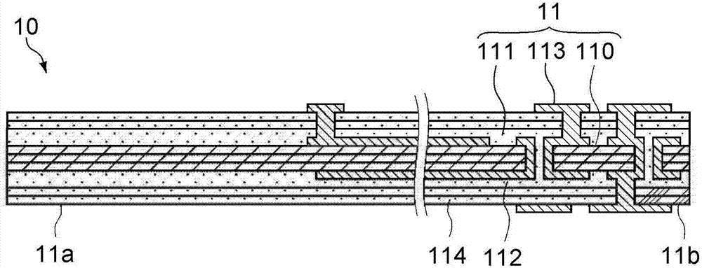
[0044] The first circuit board main body 10 is composed of a flexible wiring base 11 connecting the second circuit board main body 20 and the control circuit board 30 , and constitutes a flexible portion in the circuit board 100...

no. 2 approach >

[0084] Figure 5 It is a schematic side sectional view showing the structure of a circuit board 200 according to another embodiment of the present invention. The following description will mainly focus on the configurations different from those of the first embodiment, and the descriptions of the same configurations as those of the first embodiment will be omitted or simplified by assigning the same symbols.

[0085] The circuit board 200 of this embodiment is the same as that of the first embodiment in that it has a first circuit board body 10 and a second circuit board body 20 , but this embodiment includes electronic components 26 buried in the second circuit board body 20 This point is different from the first embodiment.

[0086] In this embodiment, the second circuit board main body 20 includes: a resin layer 21 selectively covering the first end portion 11a of the flexible wiring base material 11; a circuit portion 22 provided on the resin layer 21; The reinforcing me...

no. 3 approach >

[0093] Image 6 It is a schematic side sectional view showing the structure of a circuit board 300 according to another embodiment of the present invention. The following description will mainly focus on the configurations different from those of the first embodiment, and the descriptions of the same configurations as those of the first embodiment will be omitted or simplified by assigning the same symbols.

[0094] The circuit board 300 of this embodiment is the same as the first embodiment in that it has a first circuit board body 10 and a second circuit board body 20 , but in this embodiment, a reinforcement member 270 is embedded in the second circuit board body 20 The point that the multilayer substrate 27 is the core differs from the first embodiment.

[0095] In this embodiment, the second circuit board main body 20 includes: a resin layer 21 selectively covering the first end portion 11a of the flexible wiring base material 11; a circuit portion 22 provided on the res...


PUM


Abstract

The present invention provides a circuit board that can improve the strength of a rigid portion while satisfying thickness requirements, and a method of manufacturing the circuit board. The circuit board (100) of one aspect of the present invention includes a flexible wiring material (11) having a first end portion (11a) and a second end portion (11b) opposite to the first end portion (11a); and a reinforcement portion (12) comprising a resin layer (21) selectively covering the first end portion (11a), a circuit portion (22) disposed on the resin layer (21) and electrically connected to the flexible wiring material (11), and a metallic plate-shaped or frame-shaped reinforcement member embedded in the resin layer (21).

Description

technical field [0001] The present invention relates to a circuit board having a flexible portion and a rigid portion and a manufacturing method thereof. Background technique [0002] With the expansion of the information and communication industry, people's needs for electronic equipment have become diverse, and the need for early development and mass production has also become high. In particular, smartphones have added various functions such as Internet, e-mail, camera, GPS, wireless LAN, and ONE-SEG TV in addition to the basic functions as a telephone, and the number of models has also increased. For high-performance smartphones, increasing battery capacity is a problem, and high-density mounting of motherboards, miniaturization / thinning, and componentization of functional modules are being developed. Among them, there is a demand for thinner components mounted in smartphones, including the method of joining them to the main board. [0003] Component circuit boards use...

Claims


Application Information

Patent Timeline
IPC IPC(8): H05K1/14H05K3/36
CPCH05K1/147H05K3/361H05K2201/2009
Inventor 杉山裕一宫崎政志
Owner TAIYO YUDEN KK
Why Eureka
Try Eureka