Doped modified lead niobate-lead zirconate titanate piezoelectric ceramic and preparation method thereof
A technology of lead niobate nickelate and lead zirconate titanate, which is applied in the field of piezoelectric ceramics, can solve the problems of inability to meet the practical application requirements of high-power piezoelectric devices, low piezoelectric and dielectric properties, and achieve stable and mature preparation methods. Excellent piezoelectric performance and dielectric performance, and the effect of easy raw material acquisition
- Summary
- Abstract
- Description
- Claims
- Application Information
AI Technical Summary
Problems solved by technology
Method used
Image
Examples
Embodiment 1
[0045] The chemical formula of the lead niobate nickelate-lead zirconate titanate piezoelectric ceramic doped and modified in this implementation is:
[0046] Pb 0.90 Sr 0.10 (Ni 1 / 3 Nb 2 / 3 ) 0.20 (Zr 0.52 Ti 0.48 ) 0.80 o 3 +0.75wt%Sb 2 o 3 +y%PbO+z%NiO, wherein y=3, z=0;
Embodiment 2
[0048] The chemical formula of the lead niobate nickelate-lead zirconate titanate piezoelectric ceramic doped and modified in this implementation is:
[0049] Pb 0.90 Sr 0.10 (Ni 1 / 3 Nb 2 / 3 ) 0.20 (Zr 0.52 Ti 0.48 ) 0.80 o 3 +0.75wt%Sb 2 o 3 +y%PbO+z%NiO, wherein y=0, z=3;
Embodiment 3
[0051] The chemical formula of the lead niobate nickelate-lead zirconate titanate piezoelectric ceramic doped and modified in this implementation is:
[0052] Pb 0.90 Sr 0.10 (Ni 1 / 3 Nb 2 / 3 ) 0.20 (Zr 0.52 Ti 0.48 ) 0.80 o 3 +0.75wt%Sb 2 o 3 +y%PbO+z%NiO, wherein y=3, z=3;
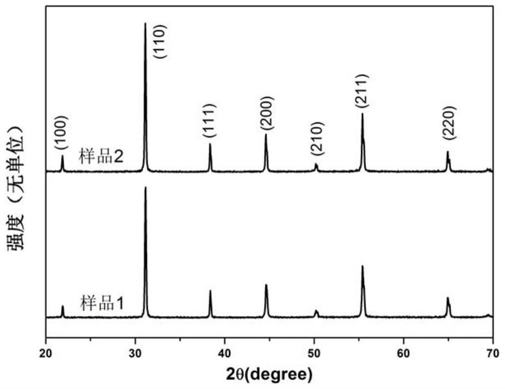
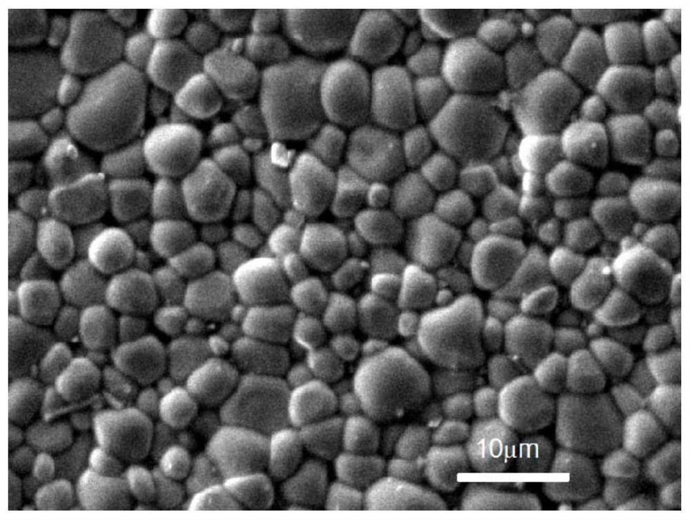
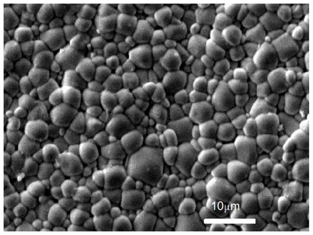
[0053] The X-ray diffraction pattern of the lead niobate nickelate-lead zirconate titanate piezoelectric ceramics prepared in this example is shown in figure 1 , SEM image see figure 2 . Depend on figure 1 It can be seen that no pyrochlore phase or second phase appears, indicating that it has a pure perovskite phase structure. Depend on figure 2 It can be seen that the grain size of the prepared materials ranges from 1 μm to 8 μm, and the grain distribution is uniform, the grain boundaries are clearly visible, the porosity is relatively small, and the ceramic structure is relatively dense.
[0054] d 33 , ε r and Q(Q=d 33 ×ε r ) change map see Figure 4 . from Figure 4 It can be s...
PUM
| Property | Measurement | Unit |
|---|---|---|
| piezoelectric charge coefficient | aaaaa | aaaaa |
| relative permittivity | aaaaa | aaaaa |
Abstract
Description
Claims
Application Information


